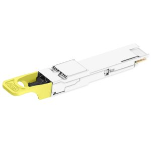
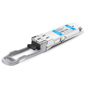

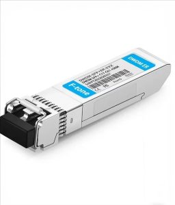
产品特点 / Product Features
- Operating data rate up to 25.78Gbps
- Up to 40km transmission distance
- High sensitivity APD photodiode and TIA
- Rate Adaptation
- LC single connector
- Hot pluggable 20pin connector
- Low power consumption <1.5 W
- Single +3.3V±5% power supply
- Compliant with SFF-8472
- Fully RoHS Compliant
- Operating temperature range:
- Commercial: 0°C to +70°C
- Industrial: -40°C to +85°C
应用场景 / Application
25GE BASE-LR Ethernet
CPRI Option 10/eCPRI
产品概述 / Description
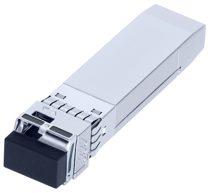
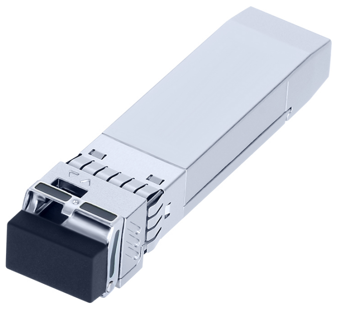
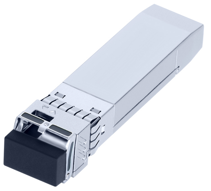
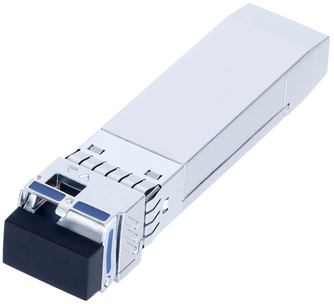
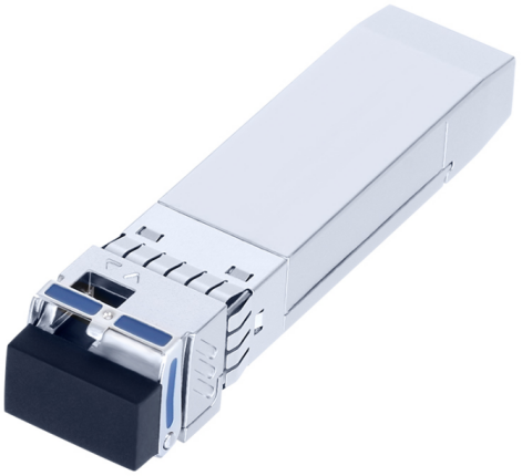
The FTCS-BxxA25G-40Dxx Transceiver is intended for 40km reach service from 24.33Gb/s to 25.78Gb/s BI-direction single mode high-speed communications equipment where low-cost, extraordinary performance and reliability are essential. It consumes low power, operates base on 3.3V DC power supply and is offered in the industrial temperature range. They are compliant with SFP28 MSA, SFF-8431 and SFF-8432.
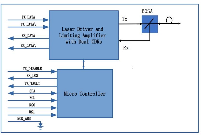
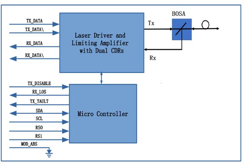
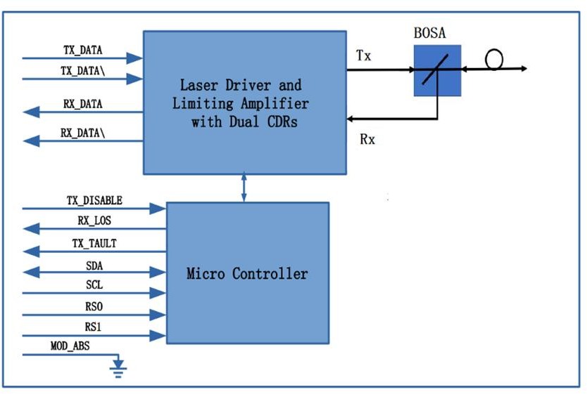
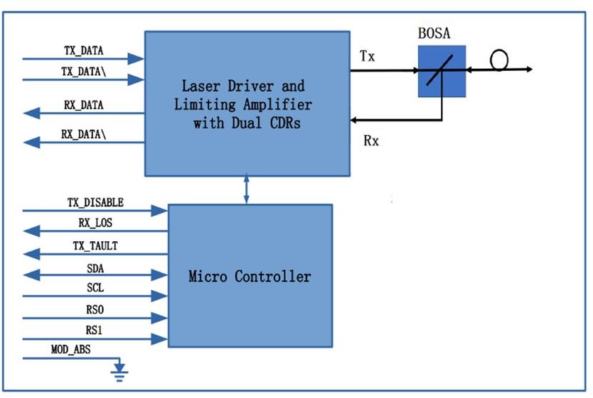
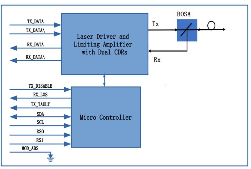
The low jitter and low bit error rate optical assembly features a DML laser transmitter and APD/TIA receiver. It utilizes internal clock and data recovery (CDR) units on transmitter and the receiver chains for low jitter compliance. The differential AC coupled Tx and Rx data interfaces are CML compatible. The device is Class I laser safety compliant.
技术参数 / Specifications
绝对最大额定值 / Absolute Maximum Ratings
| Parameter | Symbol | Unit | Min | Max |
|---|---|---|---|---|
| Storage Temperature Range | Ts | oC | -40 | 85 |
| Relative Humidity | RH | % | 0 | 85 |
推荐工作条件 / Recommended Operating Conditions
| Parameter | Symbol | Unit | Min | Typ | Max |
|---|---|---|---|---|---|
| Operating Case Temperature Range | Tc | oC | -40 | 85 | |
| Power Supply Voltage | Vcc | V | 3.14 | 3.3 | 3.46 |
| Bit Rate | BR | Gb/s | 25.78 | ||
| Bit Error Ratio | BER | 5*10-5 | |||
| Max Supported Link Length | L | Km | 40 |
电接口定义 / Electric Ports Definition
| Parameter | Symbol | Unit | Min | Typ | Max | Note |
|---|---|---|---|---|---|---|
| Transmitter | ||||||
| Input Differential Impedance | RIN | Ω | 100 | |||
| Single-ended Data Input Swing | VIN | mVp-p | 90 | 450 | ||
| Transmit Disable Voltage | VDIS | V | 2 | VCCHOST | ||
| Transmit Enable Voltage | VEN | V | VEE | VEE+0.8 | ||
| Transmit Fault Assert Voltage | VFA | V | 2 | VCCHOST | ||
| Transmit Fault De-Assert Voltage | VFDA | V | VEE | VEE+0.4 | ||
| Receiver | ||||||
| Single-ended Data Output Swing | VOD | mVp-p | 200 | 450 | ||
| LOS Fault | VLOSFT | V | 2 | VCCHOST | ||
| LOS Normal | VLOSNR | V | VEE | VEE+0.4 | ||
光学特性 / Optical Characteristics
| Parameter | Symbol | Unit | Min | Typ | Max | Note |
|---|---|---|---|---|---|---|
| Transmitter | ||||||
| Center Wavelength (FTCS-B27A25G-40Dxx) | λ | nm | 1260 | 1270 | 1280 | |
| Center Wavelength (FTCS-B13A25G-40Dxx) |
λ | nm | 1300 | 1310 | 1320 | |
| Average Output Power | Pav | dBm | 0 | 6 | ||
| Spectral Width (-20dB) | nm | 1 | ||||
| Extinction Ratio | ER | dB | 3.5 | |||
| Side Mode Suppression Ratio | SMSR | dB | 30 | |||
| Average Launch Power of OFF Transmitter | POFF | dBm | -30 | |||
| Relative Intensity Noise | RIN | dB/Hz | -128 | |||
| Receiver | ||||||
| Center Wavelength (FTCS-B13A25G-40Dxx) | λC | nm | 1300 | 1310 | 1320 | |
| Center Wavelength (FTCS-B27A25G-40Dxx) |
λC | nm | 1260 | 1270 | 1280 | |
| Receiver Sensitivity(OMA) | RSENSE | dBm | -19 | 1 | ||
| Receiver Overload (OMA) | Pmax | dBm | -5 | |||
| Receiver Reflectance | dB | -12 | ||||
| LOS Assert | LOSA | dBm | -35 | |||
| LOS De-Assert LOS | LOSD | dBm | -21 | |||
| LOS Hysteresis | dB | 0.5 | ||||
Note1: Measured at 25.78125Gb/s, ER>3.5dBm, PRBS 231-1 and BER better than or equal to 5E-5;
引脚定义 / Pin Assignment
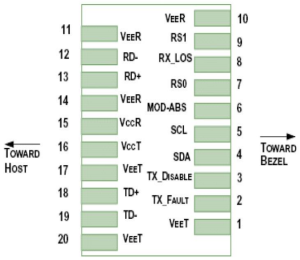
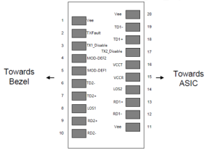
Figure 1.Pin function definitions
Table 1: Transceiver pin descriptions
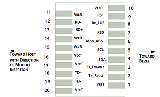
| Pin Number | Symbol | Name | Description |
|---|---|---|---|
| 1,17,20 | VeeT | Transmitter Signal Ground | Connected to signal ground on the host board. |
| 2 | TX Fault | Transmitter Fault Out (OC) | Module transmitter fault output. |
| 3 | TX Disable | Transmitter Disable In (LVTTL) | Module transmitter disable control. |
| 4 | SDA | Module Definition Identifiers | Serial ID with SFF 8472 Diagnostics Module Definition pins should be pulled up to Host Vcc with 10 kΩ resistors. |
| 5 | SCL | ||
| 6 | MOD-ABS | ||
| 7 | RS0 | Receiver Rate Select (LVTTL) Transmitter Rate Select (LVTTL) | Rate select 0(Rx):Low=CDR Bypass ; High=CDR Select Rate select 1(Tx):Low=CDR Bypass ; High=CDR Select |
| 9 | RS1 | ||
| 8 | LOS | Loss of Signal Out (OC) | Receiver loss of signal. |
| 10,11,14 | VeeR | Receiver Signal Ground | Connected to signal ground on the host board. |
| 12 | RD- | Receiver Negative DATA Out (CML) | Receiver inverted data output, internally AC coupled and terminated |
| 13 | RD+ | Receiver Positive DATA Out (CML) | Receiver non-inverted data output, internally AC coupled and terminated. |
| 15 | VccR | Receiver Power Supply | Receiver Power 3.3V Supply. |
| 16 | VccT | Transmitter Power Supply | Transmitter Power 3.3V Supply. |
| 18 | TD+ | Transmitter Positive DATA In (CML) | Transmitter non-inverted data input, internally AC coupled and terminated. |
| 19 | TD- | Transmitter Negative DATA In (CML) | Transmitter inverted data Input, internally AC coupled and terminated. |
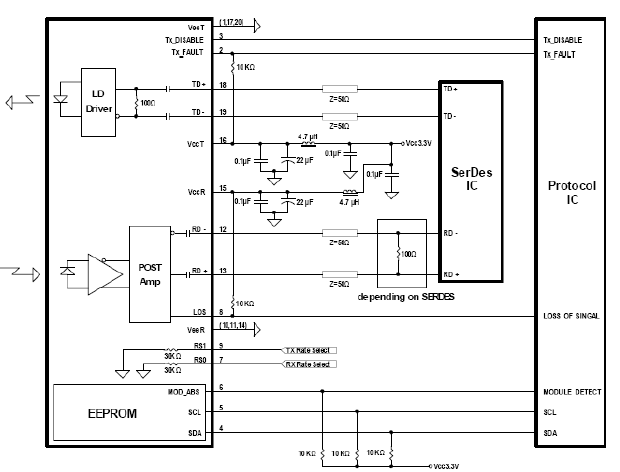
推荐接口电路 / Recommended Interface Circuit
Figure 2. Typical application circuit
机械尺寸 / Mechanical Dimensions
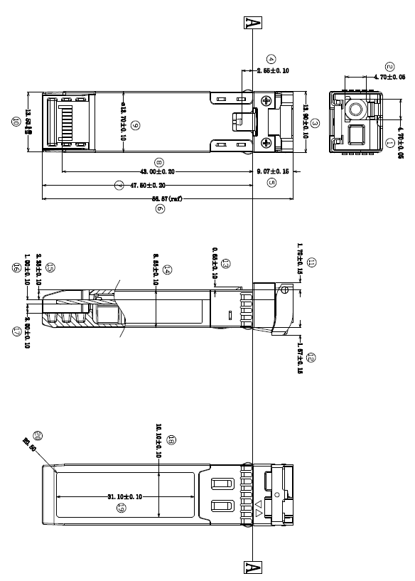
Figure 3. Module Mechanical Dimensions
数字诊断功能 / Digital Diagnostics Functions
As defined by the SFF-8472, The SFP28 transceivers provide digital diagnostic functions via a 2-wire serial interface, which allows real-time access to the following operating parameters:
Transceiver temperature
Laser bias current
Transmitted optical power
Received optical power
Transceiver supply voltage
It also provides a sophisticated system of alarm and warning flags, which may be used to alert end-users when particular operating parameters are outside of a factory-set normal range. The operating and diagnostics information is monitored and reported by a Digital Diagnostics Transceiver Controller (DDTC) inside the transceiver, which is accessed through the 2-wire serial interface. The memories are organized as a series of 8-bit data words that can be addressed individually or sequentially. The 2-wire serial interface provides sequential or random access to the 8 bit parameters, addressed from 0x00h to the maximum address of the memory. For more detailed information, including memory map definitions, please refer the SFF-8472 documentation.
数字诊断精度 / Digital Diagnostic Monitor Accuracy
The following characteristics are defined over recommended operating conditions
| Parameter | Accuracy | Unit |
|---|---|---|
| Internally measured transceiver temperature | +/-3 | deg.C |
| Internally measured transceiver supply voltage | +/-3 | % |
| Measured Tx bias current | +/-10 | % |
| Measured Tx output power | +/-3 | dB |
| Measured Rx received average optical power | +/-3 | dB |
订购信息 / Ordering Information
| Part Number | Product Description |
|---|---|
| FTCS-B27A25G-40D | 25G SFP28 40km BIDI transceiver 1270 Tx/ 1310 Rx, with DDM, 0℃~70℃ |
| FTCS-B13A25G-40D | 25G SFP28 40km BIDI transceiver 1310 Tx/ 1270 Rx, with DDM, 0℃~70℃ |
| FTCS-B27A25G-40DI | 25G SFP28 40km BIDI transceiver 1270 Tx/ 1310 Rx, with DDM, -40℃~85℃ |
| FTCS-B13A25G-40DI | 25G SFP28 40km BIDI transceiver 1310 Tx/ 1270 Rx, with DDM, -40℃~85℃ |
地区:中国四川天府新区
服务区域:全球
联系方式:
企业电话:028-85255257 | 企业传真:028-85977702 | 企业手机:19081343401
Site:https://www.f-tone.com
人事部:hr@f-tone.com | 市场部:sales@f-tone.com | 技术支持:support@f-tone.com
本产品为光模块产品线,详细信息,请联系我们的销售人员,谢谢!
Important Notice
Performance figures, data and any illustrative material provided in this data sheet are typical and must be specifically confirmed in writing by F-tone Networks before they become applicable to any particular order or contract. In accordance with the F-tone Networks policy of continuous improvement specifications may change without notice. The publication of information in this data sheet does not imply freedom from patent or other protective rights of F-tone Networks or others. Further details are available from any F-tone Networks sales representative.