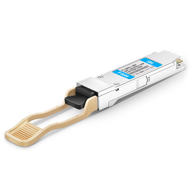
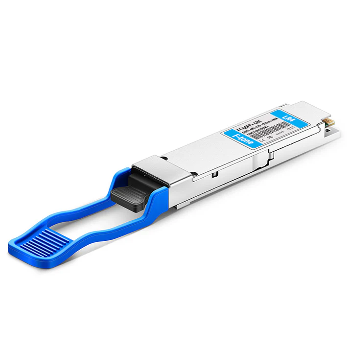
Bi-Directional, QSFP+ Pluggable, Duplex LC
40 Gigabit Ethernet Fiber-OpticsTransceiver
FTBR-79EBPZ
Applications
Description Features
The FTBR-79EBP Z is aFour-Chann el,• Compliant to the 40GbE XLPPI electrical specification
Pluggable, LC Duplex, Fiber-Optic QSFP+ Transceiver for per IEEE 802.3ba-2010
40 Gigabit Ethernet Applications. This transceiver is a high • Compliant to QSFP+ SFF-8436 Specification
performance module for short-range duplex data com-
• Power Level 4: Max Power 3.5W
munication and interconnect applications. It integrates
four electrical data lanes in each direction into transmis- • Class 1M Eye Safety
sion over a single LC duplex fiber optic cable. Each elec- • High port density: 21mm horizontal port pitch
trical lane operates at 10.3125 Gbps and conforms to the
• Operates at 10.3125 Gbps per electrical channel with
40GE XLPPI interface.
64b/66b encoded data
The FTBR-79EBPZ transceiver internally multiplexes
• Links up to 100m using OM3 and 150m using OM4
an XLPPI 4x10G interface into two 20Gb/s electrical
optical fiber
chan-nels, transmitting and receiving each optically
• +10 to +70ºC case temperature operating range
over one simplex LC fiber using bi-directional optics.
This results in an aggregate bandwidth of 40Gbps into • Proven High Reliability technology: VCSEL
a duplex LC cable. This allows reuse of the installed LC transmitters and PIN receiver
duplex cabling infrastructure for 40GbE application.
• Hot pluggable transceiver for ease of installation and
Link distances up to 100 m using OM3 and 150m using servicing
OM4 optical fiber are supported. These modules are de- • Two wire Serial (TWS) Management Interface with
signed to operate over multimode fiber systems using a maskable interrupts for expanded functionality
nominal wavelength of 850nm on one end and 900nm on
• UtilizesastandardLCduplexfibercableallowingreuse
the other end. The electrical interface uses a 38 contact
of existing cable infrastructure
QSFP+ type edge connector. The optical interface uses a
conventional LC duplex connector. This module incorpo-
rates F-tone Networks proven integrated circuit andVCS
• 40 Gigabit Ethernet interconnects
EL technology to provide reliable long life, high per-for
mance, and consistent service. • Datacom/Telecom switch & router connections
• Data aggregation and backplane applications
• Proprietary protocol and density applications
V 3.06
1 /18
WARNING
CAUTION! Viewing the laser output with certain optical instruments (for
example, eye loupes, magnifiers and microscopes) within a distance of
INVISIBLE LASER RADIATION
100 mm may pose an eye hazard.
DO NOT VIEW DIRECTLY
CAUTION! Use of controls or adjustments or performance of procedures
WITH OPTICAL INSTRUMENTS
other than those specified herein may result in hazardous radiation
CLASS 1M LASER PRODUCT exposure.
Note: Standard used for classification: EN 60825-1:2007
CLASS 1M LASER PRODUCT: INVISIBLE LASER RADIATION, DO NOT VIEW DIRECTLY WITH OPTICAL INSTRUMENTS
Figure 1. Transceiver Block Diagram
Transmitter Receiver
The optical transmitter portion of the transceiver (see Fig- The optical receiver portion of the transceiver (see Figure
ure 1) incorporates a 4-channel XLPPI input buffer, elec- 1) incorporates two high speed PIN photodiodes, TIAs,
trical multiplexer, two laser drivers and two high speed signal processors, electrical de-multiplexer and 4 chan-
VCSELs (Vertical Cavity Surface Emitting Laser). The trans- nel electrical output buffer blocks. The Rx Output Buffer
mitter is designed for EN 60825 and CDRH Class 1M eye provides XLPPI compatible differential outputs for the
safety compliance. The Tx Input Buffer provides XLPPI high speed electrical interface presenting nominal single-
compatible differential inputs presenting a nominal dif- ended output impedances of 50 Ohms to AC ground and
ferential input impedance of 100 Ohms. AC coupling 100 Ohms differentially that should be differentially termi-
capacitors are located inside the QSFP+ module and are nated with 100 Ohms. AC coupling capacitors are located
not required on the host board. For module control and inside the QSFP+ module and are not required on the host
interrogation, the control interface (LVTTL compatible) in- board.
corporates a Two Wire Serial (TWS) interface of clock and
The electrical output will squelch for loss of input signal
data signals.
(unless squelch is disabled) and channel de-activation
through TWS interface. To reduce the need for polling, a
hardware interrupt signal INTL is provided to inform hosts
of an assertion of LOS or Tx_FAULT.
40GE
XLPPI
Electrical
Interface
QSFP Electrical
Connector
Gearbox IC
Din[3:0][p/n] (8)
20G BiDi Optical
SCL
SDA
Mod Sel
LPMode
ModPresL
ResetL
IntL
20G
Dout[3:0][p/n] (8) 20G BiDi Optical
uC
LC
Duplex
Optical
Interface
20G Laser Driver + TIA
20G
VCSEL,
PIN
and
Bidirectional
optics
TX λ1
RX λ2
20G
VCSEL,
PIN
and Bidirectional
optics
TX λ2
4X10G
CDR 4:2 Mux 20G 20G
RX λ1
2X20G
2:4 DeMux
CDR 20G Laser
20G Driver + TIA
V 3.06
2 /18
Host Board
(Only 2 electrical channels/1 optical channel shown for simplicity)
ASIC (SerDes)
Figure 2. Application Reference Diagram
High Speed Electrical Signal Interface Package Outline
Figure 2 shows the interface between an ASIC/SerDes and The module is designed to meet the package outline de-
the QSFP+ module. For simplicity, only two electrical chan- fined in the QSFP+ SFF-8436 Specification. See the pack-
nels and one optical channel is shown. The high speed age outline and host board footprint figures (Figures 13
signal lines are AC-coupled 100 Ohm differential lines. The – 16) for details.
AC coupling is inside the QSFP+ module and not required
Handling
on the host board. The 100 Ohm differential terminations
are inside the QSFP+ module for the transmitter lines and
The transceiver module can be damaged by exposure to
at the host ASIC/SerDes for the Receiver lines. All transmit-
current surges and over voltage events. Care should be
ter and receiver electrical channels are compliant to mod-
taken to restrict exposure to the conditions defined in the
ule XLPPI specifications per IEEE 802.3ba.
Absolute Maximum Ratings. Wave soldering, reflow sol-
dering and/or aqueous wash process with the modules on
Control Signal Interface
board are not recommended. Normal handling precau-
The module has the following low speed signals for con- tions for electrostatic discharge sensitive devices should
trol and status: ModSelL, LPMode, ResetL, ModPrsL, IntL. be observed.
In addition, there is an industry standard two wire serial
Each module is supplied with an inserted port plug for
interface scaled for 3.3 volt LVTTL. It is implemented as a
protection of the optical ports. This plug should always be
slave device. Signal and timing characteristics are further
in place whenever a fiber cable is not inserted.
defined in the Control Interface section. The registers of
the serial interface memory are defined in the Memory The optical connector includes recessed elements that
Map section and the corresponding F-tone Networks QSF are exposed whenever a cable or port plug is not inserted.
P+ Memory Map document. Prior to insertion of a fiber optic cable, it is recommended
that the cable end be cleaned to avoid contamination
Regulatory & Compliance Issues
from the cable plug. The port plug ensures the optics re-
mains clean and no additional cleaning should be needed.
Various standard and regulations apply to the modules.
In the event of contamination, standard LC port cleaning
These include eye-safety, EMC, ESD and RoHS. See the
method may be used.
Regulatory Section for details regarding these and com-
ponent recognition. Please note the transmitter module
is a Class 1M laser product – DO NOT VIEW RADIATION
DIRECTLY WITH OPTICAL INSTRUMENTS. See Regulatory
Compliance Table for details.
rotcennoC
draC
egdE
tsoH
egdE
draC
eludoM
1:2 20G
De-Mux Rx
2:1 20G
Mux Tx
)ecafretnI
tsoH(
troP/rotcennoC
lacitpO
)ecafretnI
lacitpO(
V 3.06
3 /18
Absolute Maximum Ratings
Stress in excess of any of the individual Absolute Maximum Ratings can cause immediate catastrophic damage to the
module even if all other parameters are within Recommended Operating Conditions. It should not be assumed that
limiting values of more than one parameter can be applied to the module concurrently. Exposure to any of the Absolute
Maximum Ratings for extended periods can adversely affect reliability.
Parameter Symbol Min Max Units Reference
Storage Temperature TS -40 85 °C
3.3 V Power Supply Voltage VCC -0.5 3.6 V
Data Input Voltage – Single Ended -0.5 VCC+0.5 V
Data Input Voltage – Differential |Vdip – Vdin| 1.0 V
Control Input Voltage Vi -0.5 VCC+0.5, 3.6 V
Control Output Current IO -20 20 mA
Relative Humidity RH 5 95 %
Note:
1. This is the maximum voltage that can be applied across the differential inputs without damaging the input circuitry.
Recommended Operating Conditions
Recommended Operating Conditions specify parameters for which the optical and electrical characteristics hold un-
less otherwise noted. Optical and electrical characteristics are not defined for operation outside the Recommended
Operating Conditions where reliability is not implied and damage to the module may occur for such operation over an
extended period of time.
Parameter Symbol Min Typ Max Units Reference
Case Temperature TC +10 +70 °C 1
3.3 V Power Supply Voltage VCC 3.1 3.3 3.47 V
Signal Rate per Electrical Channel (4 x 10GBd) 10.3125 GBd 2
Signal Rate per Optical Channel (2 x 20GBd) 20.625 GBd 2
Control* Input Voltage High Vih 2 VCC+.3 V
Control* Input Voltage Low Vil -0.3 0.8 V
Two Wire Serial (TWS) Interface Clock Rate 400 kHz
Power Supply Noise 50 mVpp 3
Receiver Differential Data Output Load 100 Ω
Fiber Length for OM3 0.5 100 m 4
Fiber Length for OM4 0.5 150 m 4
* Control signals, LVTTL (3.3 V) compatible
Note:
1. The position of case temperature measurement is shown in Figure 8.
2. 64b/66b encoding is assumed.
3. Power Supply Noise is defined as the peak-to-peak noise amplitude over the frequency range at the host supply side of the recommended power
supply filter with the module and recommended filter in place. Voltage levels including peak-to-peak noise are limited to the recommended
operating range of the associated power supply. See Figure 9 for recommended power supply filter.
4. Connection and splice loss of 1.5dB is allocated. Modal Bandwidth for OM3 fiber: 2000 MHz.km for 850nm channel, 1400MHz.km for 900nm
channel. Modal Bandwidth for OM4 fiber: 3700 MHz.km for 850nm channel, 1500MHz.km for 900nm channel.
V 3.06
4 /18
Transceiver Electrical Characteristics*
The following characteristics are defined over the Recommended Operating Conditions unless otherwise noted. Typical
values are for Tc = 40˚C, Vcc = 3.3 V
Parameter Symbols Min Typ Max Units Reference
Transceiver Power Consumption 3.5 W
Transceiver Power Supply Current 1150 mA
Transceiver Power On Initialization Time tPWR INIT 2000 ms 1
* For control signal timing including ModSelL, LPMode, ResetL, ModPrsL, IntL, SCL and SDA see Control Interface Section.
Note:
1. Power On Initialization Time is the time from when the supply voltages reach and remain above the minimum Recommended Operating Conditions
to the time when the module enables TWS access. The module at that point is fully functional.
Transmitter Electrical Characteristics