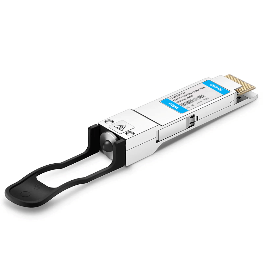
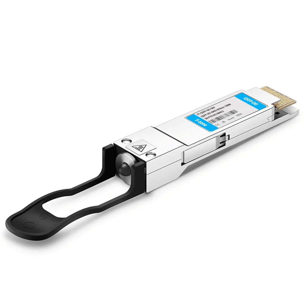
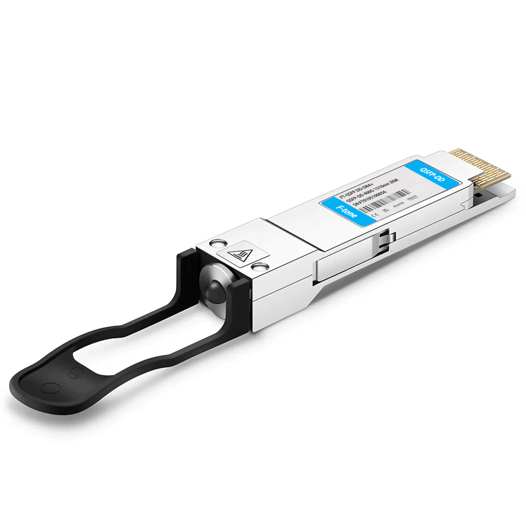
FTQD-2H-SR8
FEATURES:
- Up to 28.05 Gbps data rate per channel by NRZ modulation
- Support 200GAUI-8 electrical interface
- Integrated 850nm VCSEL array and PD array
- Hot-pluggable QSFP-DD form factor
- Supported MPO-16 APC or 2*MPO-12 UPC
- Compliant to QSFP-DD HW
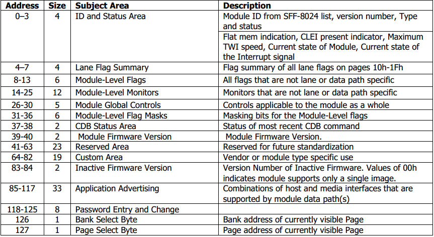
- Compliant with CMIS 4.0
- Maximum power consumption 3.5W
- Single 3.3V power supply
- Case operating temperature 0°C to 70°C
- Class 1 laser
- RoHS compliant
|
Parameter |
Symbol |
Min |
Max |
Unit |
Notes |
|
Storage Temperature |
TS |
-40 |
85 |
ºC |
|
|
Power Supply Voltage |
VCC |
-0.3 |
3.6 |
V |
|
|
Control Input Voltage |
VI |
-0.3 |
3.465 |
V |
|
|
Relative Humidity (non-condensing) |
RH |
15 |
85 |
% |
- Recommended Operating Conditions
|
Parameter |
Symbol |
Min. |
Typical |
Max. |
Unit |
Notes |
|
Operating Case Temperature |
TOPR |
0 |
– |
70 |
ºC |
|
|
Power Supply Voltage |
VCC |
3.135 |
3.3 |
3.465 |
V |
|
|
Maximum Power Consumption |
Pmax |
3.5 |
W |
|||
|
Signaling Rate per Lane |
SRL |
1.25- |
28.05 |
Gbps |
1 |
|
|
Rx Differential Data Output Load |
– |
– |
100 |
– |
Ohm |
|
|
Operating Distance (OM3) |
– |
– |
70 |
m |
||
|
Operating Distance (OM4) |
– |
– |
100 |
m |
Notes:
- For Rate <25.78 Gb/s, CDR must be in Bypass mode
- Transmitter Optical Specifications
|
Parameter |
Symbol |
Min. |
Typical |
Max. |
Unit |
Notes |
|
Center Wavelength |
λC |
840 |
850 |
860 |
nm |
|
|
RMS spectral width |
∆λrms |
0.6 |
nm |
|||
|
Average launch power, each lane |
AOPL |
-6.4 |
3 |
dBm |
||
|
Optical Modulation Amplitude (OMAouter), each lane |
TOMA |
-6.4 |
3.5 |
dBm |
||
|
Average Launch Power of OFF Transmitter, each lane |
ToFF |
-30 |
dBm |
|||
|
Extinction ratio, each lane |
ER |
2 |
– |
– |
dB |
|
|
Optical return loss tolerance |
– |
– |
-12 |
dB |
||
|
Transmitter Eye mask definition Eye mask definition {X1, X2, X2, Y1, Y2, Y3} |
{0.3,0.38,0.45,0.35,0.41,0.5} |
|||||
- Receiver Optical Specifications
|
Parameter |
Symbol |
Min. |
Typical |
Max. |
Unit |
Notes |
|
Center Wavelength |
λC |
840 |
– |
860 |
nm |
|
|
Damage threshold |
3.4 |
dBm |
||||
|
Average Receive Power, each lane |
-10.3 |
2.4 |
dBm |
|||
|
Stressed Receiver sensitivity (OMA) |
SOMA |
-5.2 |
dBm |
|||
|
Receiver reflectance |
-12 |
dB |
||||
|
LOS Assert |
LOSA |
-30 |
dBm |
|||
|
LOS De-Assert |
LOSD |
-10.5 |
dBm |
|||
|
LOS Hysteresis |
LOSH |
0.5 |
dB |
- Pin Definitions

Figure 1 –Module Pad Layout
|
Pin # |
Logic |
Symbol |
Description |
Pin # |
Logic |
Symbol |
Description |
|
1 |
GND |
Ground |
39 |
GND |
Ground |
||
|
2 |
CML-I |
Tx2n |
Transmitter Inverted Data Input |
40 |
CML-I |
Tx6n |
Transmitter Inverted Data Input |
|
3 |
CML-I |
Tx2p |
Transmitter Non-inverted Data Input |
41 |
CML-I |
Tx6p |
Transmitter Non-inverted Data Input |
|
4 |
GND |
Ground |
42 |
GND |
Ground |
||
|
5 |
CML-I |
Tx4n |
Transmitter Inverted Data Input |
43 |
CML-I |
Tx8n |
Transmitter Inverted Data Input |
|
6 |
CML-I |
Tx4p |
Transmitter Non-inverted Data Input |
44 |
CML-I |
Tx8p |
Transmitter Non-inverted Data Input |
|
7 |
GND |
Ground |
45 |
GND |
Ground |
||
|
8 |
LVTTL-I |
ModSelL |
Module Select |
46 |
Reserved |
||
|
9 |
LVTTL-I |
ResetL |
Module Reset |
47 |
VS1 |
Module Vendor Specific 1 |
|
|
10 |
VccRx |
+3.3V Power Supply Receiver |
48 |
VccRx1 |
3.3V Power Supply |
||
|
11 |
LVCMOS -I/O |
SCL |
2-wire serial interface clock |
49 |
VS2 |
Module Vendor Specific 2 |
|
|
12 |
LVCMOS -I/O |
SDA |
2-wire serial interface data |
50 |
VS3 |
Module Vendor Specific 3 |
|
|
13 |
GND |
Ground |
51 |
GND |
Ground |
||
|
14 |
CML-O |
Rx3p |
Receiver Non-inverted Data Output |
52 |
CML-O |
Rx7p |
Receiver Non-inverted Data Output |
|
15 |
CML-O |
Rx3n |
Receiver Inverted Data Output |
53 |
CML-O |
Rx7n |
Receiver Inverted Data Output |
|
16 |
GND |
Ground |
54 |
GND |
Ground |
||
|
17 |
CML-O |
Rx1p |
Receiver Non-inverted Data Output |
55 |
CML-O |
Rx5p |
Receiver Non-inverted Data Output |
|
18 |
CML-O |
Rx1n |
Receiver Inverted Data Output |
56 |
CML-O |
Rx5n |
Receiver Inverted Data Output |
|
19 |
GND |
Ground |
57 |
GND |
Ground |
||
|
20 |
GND |
Ground |
58 |
GND |
Ground |
||
|
21 |
CML-O |
Rx2n |
Receiver Inverted Data Output |
59 |
CML-O |
Rx6n |
Receiver Inverted Data Output |
|
22 |
CML-O |
Rx2p |
Receiver Non-inverted Data Output |
60 |
CML-O |
Rx6p |
Receiver Non-inverted Data Output |
|
23 |
GND |
Ground |
61 |
GND |
Ground |
||
|
24 |
CML-O |
Rx4n |
Receiver Inverted Data Output |
62 |
CML-O |
Rx8n |
Receiver Inverted Data Output |
|
25 |
CML-O |
Rx4p |
Receiver Non-inverted Data Output |
63 |
CML-O |
Rx8p |
Receiver Non-inverted Data Output |
|
26 |
GND |
Ground |
64 |
GND |
Ground |
||
|
27 |
LVTTL-O |
ModPrsL |
Module Present |
65 |
NC |
Not connected |
|
|
28 |
LVTTL-O |
IntL |
Interrupt |
66 |
Reserved |
||
|
29 |
VccTx |
+3.3V Power Supply Transmitter |
67 |
VccTx1 |
3.3V Power Supply |
||
|
30 |
Vcc1 |
+3.3V Power Supply |
68 |
Vcc2 |
3.3V Power Supply |
||
|
31 |
LVTTL-I |
InitMode |
Initialization mode |
69 |
Reserved |
||
|
32 |
GND |
Ground |
70 |
GND |
Ground |
||
|
33 |
CML-I |
Tx3p |
Transmitter Non-inverted Data Input |
71 |
CML-I |
Tx7p |
Transmitter Non-inverted Data Input |
|
34 |
CML-I |
Tx3n |
Transmitter Inverted Data Input |
72 |
CML-I |
Tx7n |
Transmitter Inverted Data Input |
|
35 |
GND |
Ground |
73 |
GND |
Ground |
||
|
36 |
CML-I |
Tx1p |
Transmitter Non-inverted Data Input |
74 |
CML-I |
Tx5p |
Transmitter Non-inverted Data Input |
|
37 |
CML-I |
Tx1n |
Transmitter Inverted Data Input |
75 |
CML-I |
Tx5n |
Transmitter Inverted Data Input |
|
38 |
GND |
Ground |
76 |
GND |
Ground |