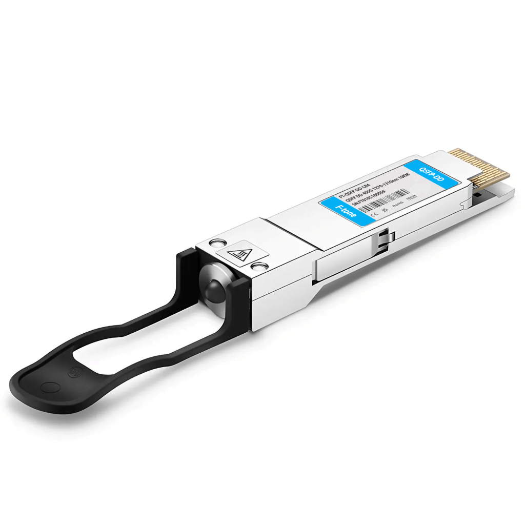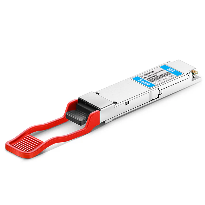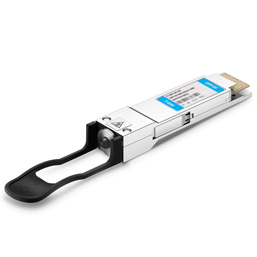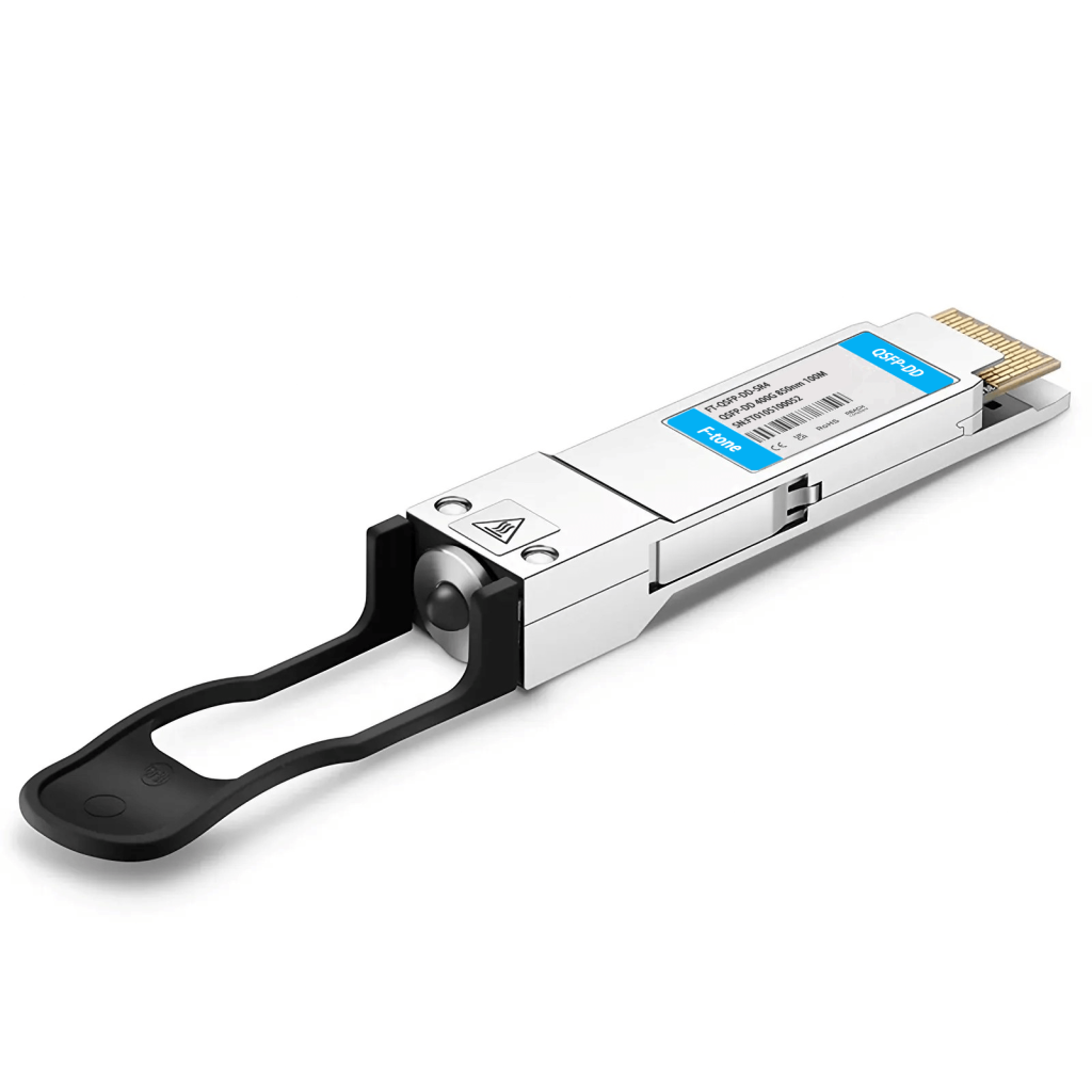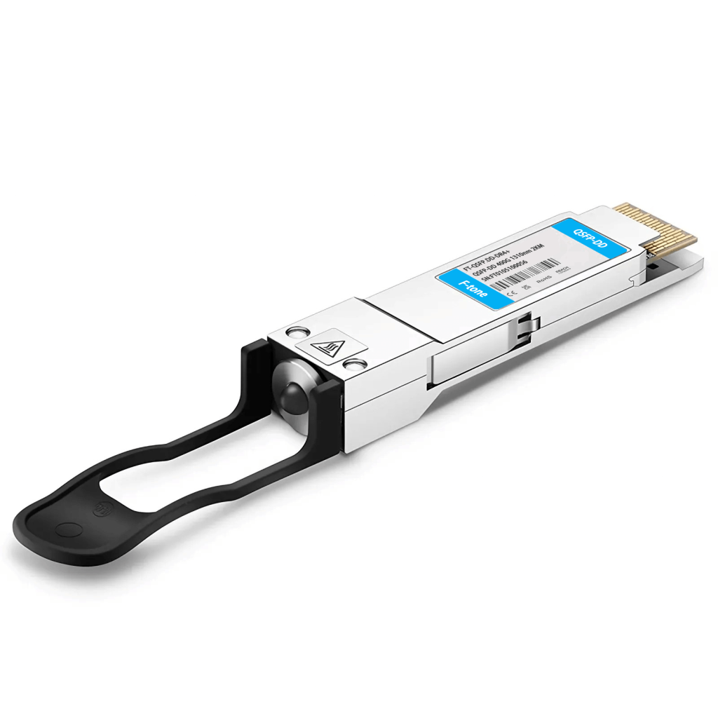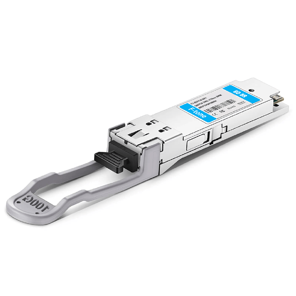
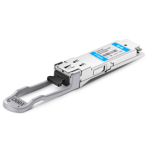

The F-tone Networks FTQD-2H-PSM4-10KM is an Four-Channel, Pluggable, Parallel, Fiber-Optic QSFP Double Density for 200Gigabit Ethernet Applications. This transceiver is a high performance module for multi-lane data communication and interconnection applications. Each lane can operate at 53.125Gbps up to 10km using G.652 SMF with KP-FEC. The electrical interface 200GAUI-8(noFEC)1 uses a 76 contact edge type connector. These modules are designed to operate over single mode fiber systems using a nominal wavelength of 1310nm. The optical interface uses a MPO12/MTP12 APC connector. This module can convert 8 channels of 25Gbps(NRZ) electrical input data to 4 channels of 50Gbps(PAM4) optical signal, and also can convert 4 channels of 50Gbps(PAM4) optical signal to 8 channels of 25Gbps (NRZ) electrical output data.The Common Management Interface Specification (CMIS) for QSFP DD modules. This module incorporates F-tone Networks proven circuit and silicon photonics technology to provide reliable long life, high performance, and consistent service.
Note:
1. KR-FEC is optional, please contact us if necessary.
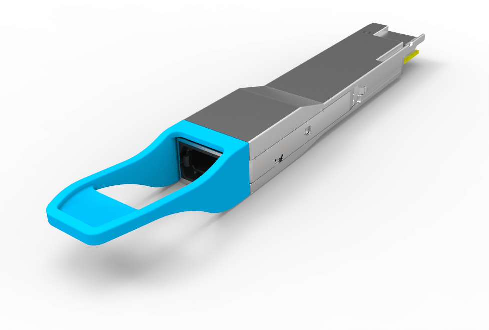
FTQD-2H-PSM4-10KM 200G QSFP-DD PSM4 光模块产品实物图
产品特性 / Features
- 4 channels full-duplex transceiver modules
- Transmission data rate up to 53Gbps per channel
- 8×25.78125Gbps NRZ transmitter and NRZ receiver
- Power consumption <9.5W
- Hot Pluggable QSFP DD form factor and Compliant with CMIS 4.0
- Maximum link length of 10km G.652 SMF with KP-FEC
- MPO12 APC connector receptacle
- Built-in digital diagnostic functions
- Operating case temperature 0°C to +70°C
- 3.3V power supply voltage
- RoHS compliant(lead free)
应用领域 / Applications
- IEEE 802.3bs 200GBASE-DR4
- Data center network
模块框图 / Module Block Diagram
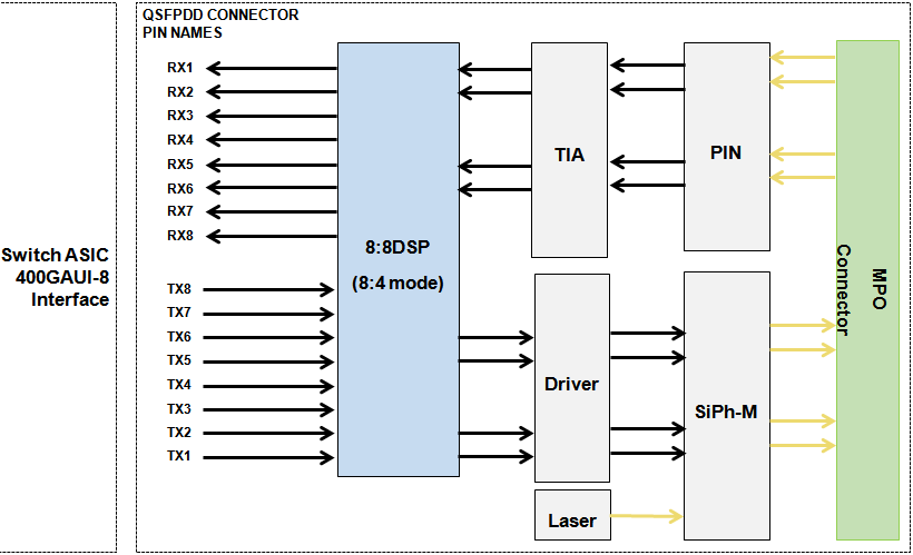
Figure1. Module Block Diagram
绝对最大额定值 / Absolute Maximum Ratings
| Parameter | Symbol | Min | Max | Unit |
|---|---|---|---|---|
| Supply Voltage | Vcc | -0.3 | 3.6 | V |
| Input Voltage | Vin | -0.3 | Vcc+0.3 | V |
| Storage Temperature | Tst | -20 | 85 | ºC |
| Case Operating Temperature | Top | 0 | 70 | ºC |
| Humidity(non-condensing) | Rh | 5 | 95 | % |
推荐工作条件 / Recommended Operating Conditions
| Parameter | Symbol | Min | Typical | Max | Unit |
|---|---|---|---|---|---|
| Supply Voltage | Vcc | 3.13 | 3.3 | 3.47 | V |
| Operating Case temperature | Tca | 0 | 70 | ºC | |
| Signal Rate per Electrical Channel (8 x 25G) |
– | 25.78125 | – | Gbps | |
| Signal Rateper Optical Channel (4 x53G) |
– | 53.125 | – | Gbps | |
| Humidity | Rh | 5 | 85 | % | |
| Power Dissipation | Pm | 9.5 | W |
电气特性 / Electrical Specifications
| Parameter | Symbol | Min | Typical | Max | Unit |
|---|---|---|---|---|---|
| Differential input impedance | Zin | 90 | 100 | 110 | ohm |
| Differential Output impedance | Zout | 90 | 100 | 110 | ohm |
| Differential input voltage amplitude | ΔVin | 900 | 1200 | mVp-p | |
| Differential output voltage amplitude | ΔVout | 1100 | mVp-p | ||
| Skew | Sw | 300 | ps | ||
| Bit Error Rate | BER | 2.4E-4 | – | ||
| Near-end Eye Width at 10^-6 probability(EW6) | 0.265 | UI | |||
| Near-end Eye Height at 10^-6 probability(EH6) | 70 | mV | |||
| Far-end Eye Width at 10^-6 probability(EW6) | 0.20 | UI | |||
| Far-end Eye Height at 10^-6 probability(EH6) | 30 | mV | |||
| Near-end Eye Linearity | 0.85 | – |
Note:
1. Differential input voltage amplitude is measured between TxnP and TxnN.
2. Differential output voltage amplitude is measured between RxnP and RxnN.
光学特性 / Optical Characteristics
发射端 / Transmitter
| Parameter | Symbol | Min | Typical | Max | Unit | Notes |
|---|---|---|---|---|---|---|
| Centre Wavelength | λc | 1304.5 | — | 1317.5 | nm | – |
| Side-mode suppression ratio | SMSR | 30 | – | — | dB | – |
| Average launch power, each lane | Pout | -5.1 | – | 3 | dBm | – |
| Optical Modulation Amplitude (OMAouter), each lane |
OMA | -3 | 2.8 | dBm | – | |
| Transmitter and dispersion eye closure(TDEC),each lane | TDEC | 3.4 | dB | |||
| Extinction Ratio | ER | 3.5 | – | – | dB | – |
| Average launch power of OFF transmitter, each lane |
-16 | dB | – |
接收端 / Receiver
| Parameter | Symbol | Min | Typical | Max | Unit | Notes |
|---|---|---|---|---|---|---|
| Centre Wavelength | λc | 1304.5 | — | 1317.5 | nm | – |
| Receiver Sensitivity in OMA outer | RXsen | -6.6 | dBm | 1 | ||
| Stressed Receiver Sensitivity in OMA outer | SRS | -4.1 | dBm | 1 | ||
| Average power at receiver , each lane input, each lane |
Pin | -8.1 | 3 | dBm | – | |
| Receiver Reflectance | -12 | dB | – | |||
| LOS Assert | -10 | dBm | – | |||
| LOS De-Assert – OMA | -7.5 | dBm | – | |||
| LOS Hysteresis | 0.5 | dB | – |
Note: Measured with conformance test signal at TP3 for BER = 2.4E-4 Pre-FEC
引脚定义 / Pin Description
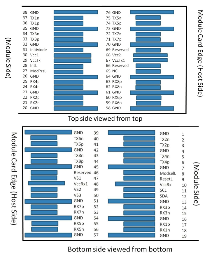
表 1 焊盘功能定义 / Pad Function Definition(上排 1~38)
| Pad | Logic | Symbol | Description | Plug Sequence | Notes |
|---|---|---|---|---|---|
| 1 | GND | Ground | 1B | 1 | |
| 2 | CML-I | Tx2n | Transmitter Inverted Data Input | 3B | |
| 3 | CML-I | Tx2p | Transmitter Non-Inverted Data Input | 3B | |
| 4 | GND | Ground | 1B | 1 | |
| 5 | CML-I | Tx4n | Transmitter Inverted Data Input | 3B | |
| 6 | CML-I | Tx4p | Transmitter Non-Inverted Data Input | 3B | |
| 7 | GND | Ground | 1B | 1 | |
| 8 | LVTTL-I | ModSelL | Module Select | 3B | |
| 9 | LVTTL-I | ResetL | Module Reset | 3B | |
| 10 | VccRX | +3.3V Power Supply Receiver | 2B | 2 | |
| 11 | LVCMOS-I/O | SCL | 2-wire serial interface clock | 3B | |
| 12 | LVCMOS-I/O | SDA | 2-wire serial interface data | 3B | |
| 13 | GND | Ground | 1B | 1 | |
| 14 | CML-O | Rx3p | Receiver Non-Inverted Data Output | 3B | |
| 15 | CML-O | Rx3n | Receiver Inverted Data Output | 3B | |
| 16 | GND | Ground | 1B | 1 | |
| 17 | CML-O | Rx1p | Receiver Non-Inverted Data Output | 3B | |
| 18 | CML-O | Rx1n | Receiver Inverted Data Output | 3B | |
| 19 | GND | Ground | 1B | 1 | |
| 20 | GND | Ground | 1B | 1 | |
| 21 | CML-O | Rx2n | Receiver Inverted Data Output | 3B | |
| 22 | CML-O | Rx2p | Receiver Non-Inverted Data Output | 3B | |
| 23 | GND | Ground | 1B | 1 | |
| 24 | CML-O | Rx4n | Receiver Inverted Data Output | 3B | |
| 25 | CML-O | Rx4p | Receiver Non-Inverted Data Output | 3B | |
| 26 | GND | Ground | 1B | 1 | |
| 27 | LVTTL-O | ModPrsL | Module Present | 3B | |
| 28 | LVTTL-O | IntL | Interrupt | 3B | |
| 29 | VccTx | +3.3V Power supply transmitter | 2B | 2 | |
| 30 | Vcc1 | +3.3V Power supply | 2B | 2 | |
| 31 | LVTTL-I | LPMode | Low Power mode | 3B | |
| 32 | GND | Ground | 1B | 1 | |
| 33 | CML-I | Tx3p | Transmitter Non-Inverted Data Input | 3B | |
| 34 | CML-I | Tx3n | Transmitter Inverted Data Input | 3B | |
| 35 | GND | Ground | 1B | 1 | |
| 36 | CML-I | Tx1p | Transmitter Non-Inverted Data Input | 3B | |
| 37 | CML-I | Tx1n | Transmitter Inverted Data Input | 3B | |
| 38 | GND | Ground | 1B | 1 |
表 2 焊盘功能定义 / Pad Function Definition(下排 39~76)
| Pad | Logic | Symbol | Description | Plug Sequence | Notes |
|---|---|---|---|---|---|
| 39 | GND | Ground | 1A | 1 | |
| 40 | CML-I | Tx6n | Transmitter Inverted Data Input | 3A | |
| 41 | CML-I | Tx6p | Transmitter Non-Inverted Data Input | 3A | |
| 42 | GND | Ground | 1A | 1 | |
| 43 | CML-I | Tx8n | Transmitter Inverted Data Input | 3A | |
| 44 | CML-I | Tx8p | Transmitter Non-Inverted Data Input | 3A | |
| 45 | GND | Ground | 1A | 1 | |
| 46 | Reserved | For future use | 3A | 3 | |
| 47 | VS1 | Module Vendor Specific 1 | 3A | 3 | |
| 48 | VccRx1 | 3.3V Power Supply | 2A | 2 | |
| 49 | VS2 | Module Vendor Specific 2 | 3A | 3 | |
| 50 | VS3 | Module Vendor Specific 3 | 3A | 3 | |
| 51 | GND | Ground | 1A | 1 | |
| 52 | CML-O | Rx7p | Receiver Non-Inverted Data Output | 3A | |
| 53 | CML-O | Rx7n | Receiver Inverted Data Output | 3A | |
| 54 | GND | Ground | 1A | 1 | |
| 55 | CML-O | Rx5p | Receiver Non-Inverted Data Output | 3A | |
| 56 | CML-O | Rx5n | Receiver Inverted Data Output | 3A | |
| 57 | GND | Ground | 1A | 1 | |
| 58 | GND | Ground | 1A | 1 | |
| 59 | CML-O | Rx6n | Receiver Inverted Data Output | 3A | |
| 60 | CML-O | Rx6p | Receiver Non-Inverted Data Output | 3A | |
| 61 | GND | Ground | 1A | 1 | |
| 62 | CML-O | Rx8n | Receiver Inverted Data Output | 3A | |
| 63 | CML-O | Rx8p | Receiver Non-Inverted Data Output | 3A | |
| 64 | GND | Ground | 1A | 1 | |
| 65 | NC | No Connect | 3A | 3 | |
| 66 | Reserved | For future use | 3A | 3 | |
| 67 | VccTx1 | 3.3V Power Supply | 2A | 2 | |
| 68 | Vcc2 | 3.3V Power Supply | 2A | 2 | |
| 69 | LVTTL-I | ePPS | Precision Time Protocol (PTP) reference clock input | 3A | 3 |
| 70 | GND | Ground | 1A | 1 | |
| 71 | CML-I | Tx7p | Transmitter Non-Inverted Data Input | 3A | |
| 72 | CML-I | Tx7n | Transmitter Inverted Data Input | 3A | |
| 73 | GND | Ground | 1A | 1 | |
| 74 | CML-I | Tx5p | Transmitter Non-Inverted Data Input | 3A | |
| 75 | CML-I | Tx5n | Transmitter Inverted Data Input | 3A | |
| 76 | GND | Ground | 1A | 1 |
Note 1: Ground.
Note 2: +3.3V Power supply.
Note 3: For future use.
Note 4: Module Vendor Specific.
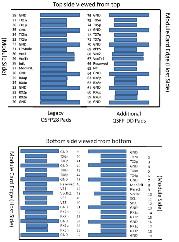
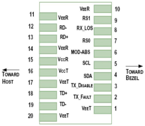
Figure2. Electrical Pin-out Details
各控制引脚说明 / Pin Function Details
ModSelL
The ModSelL is an input signal that shall be pulled to Vcc in the QSFP-DD module. When held low by the host, the module responds to 2-wire serial communication commands. The ModSelL allows the use of multiple QSFP-DD modules on a single 2-wire interface bus. When ModSelL is “High”, the module shall not respond to or acknowledge any 2-wire interface communication from the host.
In order to avoid conflicts, the host system shall not attempt 2-wire interface communications within the ModSelL de-assert time after any QSFP-DD modules are deselected. Similarly, the host must wait at least for the period of the ModSelL assert time before communicating with the newly selected module. The assertion and de-asserting periods of different modules may overlap as long as the above timing requirements are met.
ResetL
The ResetL signal shall be pulled to Vcc in the module. A low level on the ResetL signal for longer than the minimum pulse length (t_Reset_init) initiates a complete module reset, returning all user module settings to their default state.
LPMode
LPMode is an input signal. The LPMode signal shall be pulled up to Vcc in the QSFP-DD module. LPMode is used in the control of the module power mode. See CMIS Section 6.3.1.3.
ModPrsL
ModPrsL shall be pulled up to Vcc Host on the host board and pulled low in the module. The ModPrsL is asserted “Low” when the module is inserted. The ModPrsL is deasserted “High” when the module is physically absent from the host connector due to the pull-up resistor on the host board.
IntL
IntL is an output signal. The IntL signal is an open collector output and shall be pulled to Vcc Host on the host board. When the IntL signal is asserted Low it indicates a change in module state, a possible module operational fault or a status critical to the host system. The host identifies the source of the interrupt using the 2-wire serial interface. The IntL signal is deasserted “High” after all set interrupt flags are read.
电源滤波 / Power Supply Filtering
The host board should use the power supply filtering shown in Figure3.
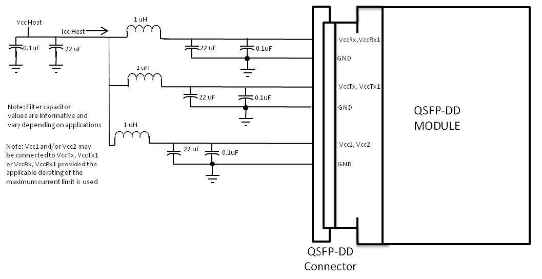
Figure3. Host Board Power Supply Filtering
光接口通道分配 / Optical Interface Lanes and Assignment
The optical interface port is a male MPO12(MTP12) APC connector.
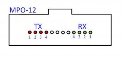
Figure 4. Optical Receptacle and Channel Orientation
数字诊断监控接口 / Diagnostic Monitoring Interface
Digital diagnostics monitoring function is available on all F-tone Networks QSFP DD products. A 2-wire serial interface provides user to contact with module.
存储结构与映射 / Memory Structure and Mapping
This limits the management memory that can be directly accessed by the host to 256 bytes, which is divided in Lower Memory (addresses 00h through 7Fh) and Upper Memory (addresses 80h through FFh).
A larger addressable management memory is required for all but the most basic modules. This is supported by a structure of 128-byte pages, together with a mechanism for dynamically mapping any of the 128-byte pages from a larger internal management memory space into Upper Memory the host addressable space.
The addressing structure of the additional internal management memory2 is shown in Figure 8-2. The management memory inside the module is arranged as a unique and always host accessible address space of 128 bytes (Lower Memory) and as multiple upper address subspaces of 128 bytes each (Pages), only one of which is selected as host visible in Upper Memory. A second level of Page selection is possible for Pages for which several instances exist (e.g. where a bank of pages with the same Page number exists).
This structure supports a flat 256 byte memory for passive copper modules and permits timely access to addresses in the Lower Memory, e.g. Flags and Monitors. Less time critical entries, e.g. serial ID information and threshold settings, are available with the Page Select function in the Lower Page. For more complex modules which require a larger amount of management memory the host needs to use dynamic mapping of the various Pages into the host addressable Upper Memory address space, whenever needed.
Note: The management memory map has been designed largely after the QSFP memory map. This memory map has been changed in order to accommodate 8 electrical lanes and to limit the required memory space. The single address approach is used as found in QSFP. Paging is used in order to enable time critical interactions between host and module.
支持的页 / Supported Pages
A basic 256 byte subset of the Management Memory Map is mandatory for all CMIS compliant devices. Other parts are only available for paged memory modules, or when advertised by the module. See CMIS V4.0 for details regarding the advertisement of supported management memory spaces.
In particular, support of the Lower Memory and of Page 00h is required for all modules, including passive copper cables. These pages are therefore always implemented. Additional support for Pages 01h, 02h and bank 0 of Pages 10h and 11h is required for all paged memory modules.
Bank 0 of pages 10h-1Fh, provides lane-specific registers for the first 8 lanes, and each additional bank provides support for additional 8 lanes. Note, however, that the allocation of information over the banks may be page specific and may not to be related to grouping data for 8 lanes.
The structure allows address space expansion for certain types of modules by allocating additional Pages. Moreover, additional banks of pages
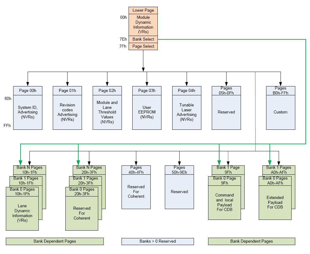
QSFP-DD Memory Map(Lower Page 与各 Page 的地址分布)
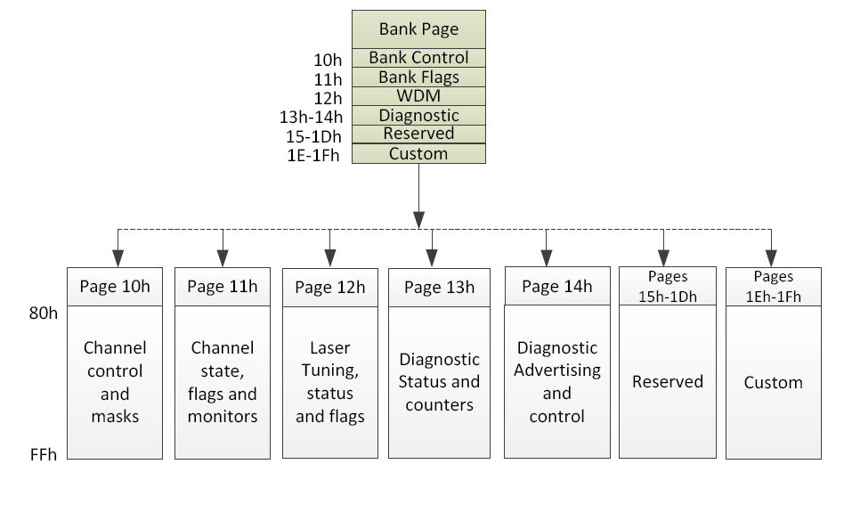
CMIS Bank Page Memory Map(Figure 8-2)
机械尺寸 / Mechanical Dimensions
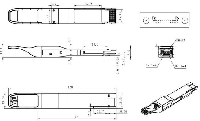
Figure6. Mechanical Specifications
法规符合性 / Regulatory Compliance
F-tone Networks FTQD-2H-PSM4-10KM transceivers are Class 1 Laser Products. They are certified per the following standards:
| Feature | Standard |
|---|---|
| Laser Safety | IEC 60825-1:2014 (Third Edition) EN60825-2:2004+A1+A2 |
| Environmental protection | 2011/65/EU |
| CE EMC | EN55032:2015 EN55035:2017 EN61000-3-2:2014 EN61000-3-3:2013 |
| FCC | FCC Part 15, Subpart B; ANSI C63.4-2014 |
| Product Safety | IEC 62368-1:2014 UL 62368-1:2014 EN 62368-1:2014 |
参考文献 / References
- QSFP DD MAS Rev5.0
- CMIS V4.0
- IEEE802.3bs 200GBASE-DR4
- OIF CEI-56G-VSR-PAM4
激光安全提示 / Laser Safety
Use of controls or adjustment or performance of procedures other than those specified herein may result in hazardous radiation exposure.
订购信息 / Ordering Information
| Part Number | Product Description |
|---|---|
| FTQD-2H-PSM4-10KM | QSFP DD, 200GBASE-DR4, 10km on Single mode Fiber (SMF),with DSP and MPO12(MTP12) APC connector. |
地区:中国四川天府新区
服务区域:全球
联系方式:
企业电话:028-85255257 | 企业传真:028-85977702 | 企业手机:19081343401
Site:https://www.f-tone.com
人事部:hr@f-tone.com | 市场部:sales@f-tone.com | 技术支持:support@f-tone.com
本产品为200G QSFP-DD 光模块产品线,详细信息,请联系我们的销售人员,谢谢!
Important Notice
Performance figures, data and any illustrative material provided in this data sheet are typical and must be specifically confirmed in writing by F-tone Networks before they become applicable to any particular order or contract. In accordance with the F-tone Networks policy of continuous improvement specifications may change without notice. The publication of information in this data sheet does not imply freedom from patent or other protective rights of F-tone Networks or others. Further details are available from any F-tone Networks sales representative.