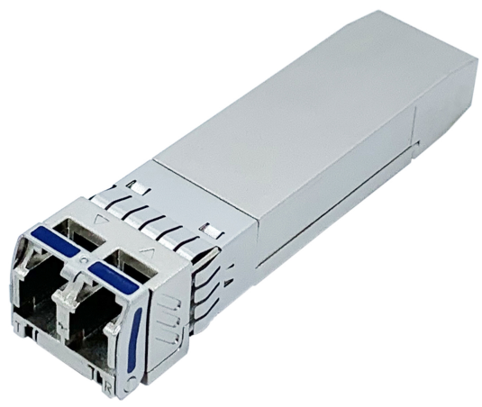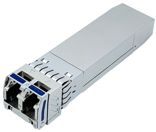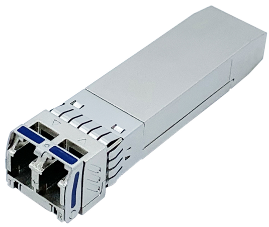

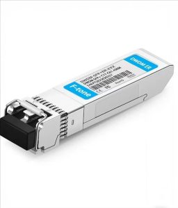
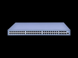
产品特点 / Product Features
- Supports up to 25.78Gbps bit rates
- Hot-pluggable SFP+ footprint
- CWDM Cooled EML laser and PIN photodiode,
- Up to 10km for SMF transmission
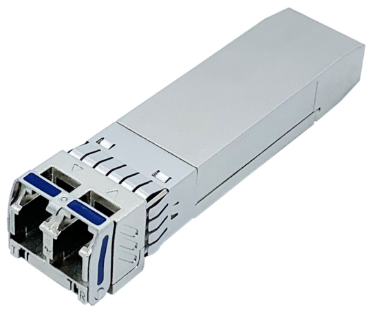
- Compliant with SFP+ MSA and SFF-8472 with duplex LC receptacle
- Compatible with RoHS
- Single +3.3V power supply
- Power dissipation <2.3W
- Real Time Digital Diagnostic Monitoring
- Operating case temperature:0 to +70°C
应用场景 / Applications
- 25G Ethernet
- CPRI 10
产品概述 / Description
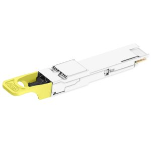
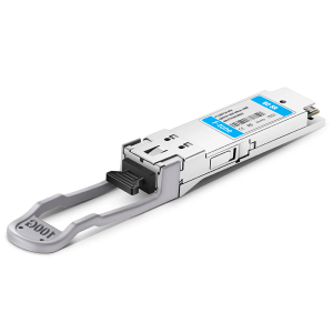
The SFP28 transceivers are high performance, cost effective modules supporting data rate of 25.78Gbps and 10km transmission distance with SMF.
The transceiver consists of three sections: a Cooled EML laser transmitter, a PIN photodiode integrated with a trans-impedance preamplifier (TIA) and MCU control unit. All modules satisfy class I laser safety requirements.
The transceivers are compatible with SFP Multi-Source Agreement and SFF-8472 digital diagnostics functions.
功能框图 / Functional Block Diagram
模块由发射、接收与控制三部分组成:发射侧由 MCU 通过 LD Bias / MOD-DEF 控制激光器驱动器(LD Driver),驱动激光器输出光信号;接收侧由光电探测器(内置跨阻放大器 TIA)与后级限幅放大器(Post Amp)恢复电信号;MCU 经 I2C(SDA/SCL)对外提供温度、电压、偏置电流、收发光功率等数字诊断信息,并处理 TX Disable、TX Fault、LOS 等控制与告警信号。
技术参数 / Specifications
绝对最大额定值 / Absolute Maximum Ratings
| Parameter | Symbol | Min | Max | Unit |
|---|---|---|---|---|
| Supply Voltage | Vcc | -0.5 | 4.5 | V |
| Storage Temperature | Ts | -40 | +85 | °C |
| Operating Humidity | – | 5 | 85 | % |
推荐工作条件 / Recommended Operating Conditions
| Parameter | Symbol | Min | Typical | Max | Unit |
|---|---|---|---|---|---|
| Operating Case Temperature | Tc | 0 | +70 | °C | |
| Power Supply Voltage | Vcc | 3.135 | 3.30 | 3.465 | V |
| Power Supply Current | Icc | 700 | mA | ||
| Data Rate | 25.78 | Gbps |
光学与电特性 / Optical and Electrical Characteristics
| Parameter | Symbol | Min | Typical | Max | Unit | Notes | ||
|---|---|---|---|---|---|---|---|---|
| Transmitter | ||||||||
| Centre Wavelength | λc | λc-6.5 | λc | λc+6.5 | nm | |||
| Spectral Width(-20dB) | Δλ | 1 | nm | |||||
| Side-Mode Suppression Ratio | SMSR | 30 | – | dB | ||||
| Average Output Power | Pout | -1 | +6 | dBm | 1 | |||
| Extinction Ratio | ER | 6 | dB | |||||
| Data Input Swing Differential | VIN | 180 | 850 | mV | 2 | |||
| Input Differential Impedance | ZIN | 90 | 100 | 110 | Ω | |||
| TX Disable | Disable | 2.0 | Vcc | V | ||||
| Enable | 0 | 0.8 | V | |||||
| TX Fault | Fault | 2.0 | Vcc | V | ||||
| Normal | 0 | 0.8 | V | |||||
| Receiver | ||||||||
| Centre Wavelength | λc | 1450 | 1620 | nm | ||||
| Receiver Sensitivity | -12 | dBm | 3 | |||||
| Receiver Overload | 2 | dBm | 3 | |||||
| LOS De-Assert | LOSD | -13 | dBm | |||||
| LOS Assert | LOSA | -35 | dBm | |||||
| LOS Hysteresis | 0.5 | dB | ||||||
| Data Output Swing Differential | Vout | 300 | 900 | mV | 4 | |||
| LOS | High | 2.0 | Vcc | V | ||||
| Low | 0.8 | V | ||||||
Notes:
1. The optical power is launched into SMF.
2. PECL input, internally AC-coupled and terminated.
3. Measured with a PRBS 231-1 test pattern @25.78Gbps, BER ≤5E-5.
4. Internally AC-coupled.
时序与电特性 / Timing and Electrical
| Parameter | Symbol | Min | Typical | Max | Unit |
|---|---|---|---|---|---|
| Tx Disable Negate Time | t_on | 1 | ms | ||
| Tx Disable Assert Time | t_off | 10 | µs | ||
| Time To Initialize, including Reset of Tx Fault | t_init | 300 | ms | ||
| Tx Fault Assert Time | t_fault | 100 | µs | ||
| Tx Disable To Reset | t_reset | 10 | µs | ||
| LOS Assert Time | t_loss_on | 100 | µs | ||
| LOS De-assert Time | t_loss_off | 100 | µs | ||
| Serial ID Clock Rate | f_serial_clock | 100 | 400 | KHz | |
| MOD_DEF (0:2)-High | VH | 2 | Vcc | V | |
| MOD_DEF (0:2)-Low | VL | 0.8 | V |
数字诊断 / Diagnostics
| Parameter | Range | Unit | Accuracy | Calibration |
|---|---|---|---|---|
| Temperature | 0 to +70 | °C | ±3°C | Internal |
| Voltage | 3.0 to 3.6 | V | ±3% | Internal |
| Bias Current | 0 to 120 | mA | ±10% | Internal |
| TX Power | -1 to +6 | dBm | ±3dB | Internal |
| RX Power | -15 to 2 | dBm | ±3dB | Internal |
数字诊断存储映射 / Digital Diagnostic Memory Map
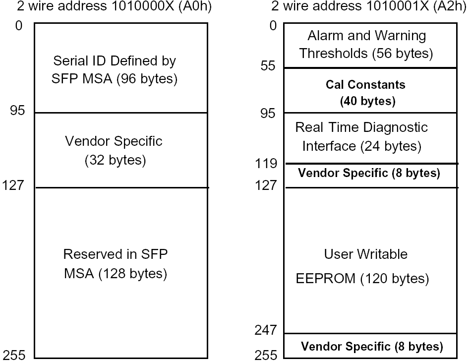
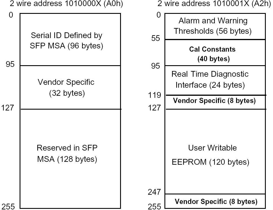
The transceivers provide serial ID memory contents and diagnostic information about the present operating conditions by the 2-wire serial interface (SCL, SDA).
The diagnostic information with internal calibration or external calibration all are implemented, including received power monitoring, transmitted power monitoring, bias current monitoring, supply voltage monitoring and temperature monitoring.
The digital diagnostic memory map specific data field defines as following.
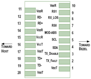
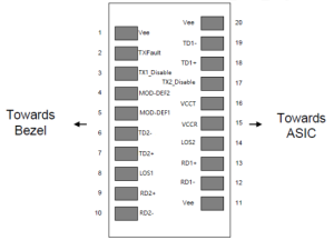
引脚定义 / Pin Descriptions
| Pin | Signal Name | Description | Plug Seq. | Notes |
|---|---|---|---|---|
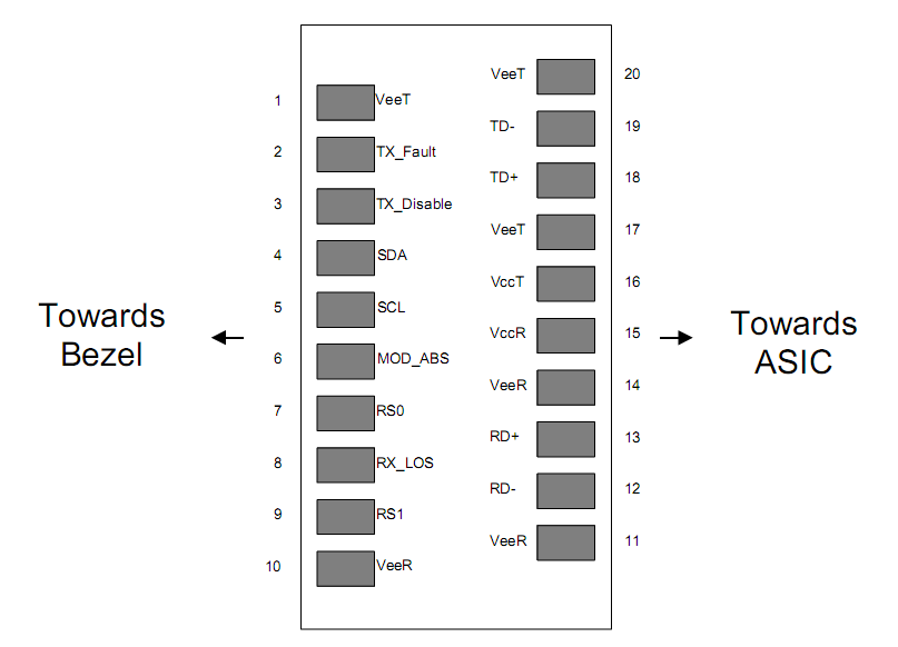
| 1 | VEET | Transmitter Ground | 1 | |
| 2 | TX FAULT | Transmitter Fault Indication | 3 | Note 1 |
| 3 | TX DISABLE | Transmitter Disable | 3 | Note 2 |
| 4 | SDA | SDA Serial Data Signal | 3 | |
| 5 | SCL | SCL Serial Clock Signal | 3 | |
| 6 | MOD_ABS | Module Absent. Grounded within the module | 3 | |
| 7 | RS0 | Not Connected | 3 | |
| 8 | LOS | Loss of Signal | 3 | Note 3 |
| 9 | RS1 | Not Connected | 3 | |
| 10 | VEER | Receiver ground | 1 | |
| 11 | VEER | Receiver ground | 1 | |
| 12 | RD- | Inv. Received Data Out | 3 | Note 4 |
| 13 | RD+ | Received Data Out | 3 | Note 4 |
| 14 | VEER | Receiver ground | 1 | |
| 15 | VCCR | Receiver Power Supply | 2 | |
| 16 | VCCT | Transmitter Power Supply | 2 | |
| 17 | VEET | Transmitter Ground | 1 | |
| 18 | TD+ | Transmit Data In | 3 | Note 5 |
| 19 | TD- | Inv. Transmit Data In | 3 | Note 5 |
| 20 | VEET | Transmitter Ground | 1 |
Notes:
Plug Seq.: Pin engagement sequence during hot plugging.
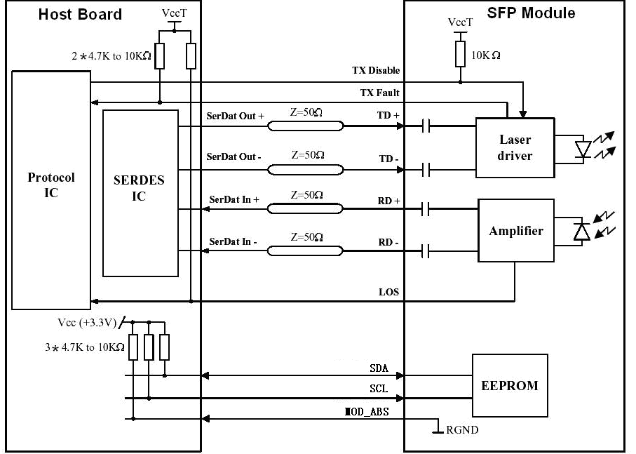
1) TX Fault is an open collector output, which should be pulled up with a 4.7k~10kΩ resistor on the host board to a voltage between 2.0V and Vcc+0.3V. Logic 0 indicates normal operation; Logic 1 indicates a laser fault of some kind. In the low state, the output will be pulled to less than 0.8V.
2) Laser output disabled on TDIS >2.0V or open, enabled on TDIS <0.8V.
3) LOS is open collector output. Should be pulled up with 4.7k~10kΩ on host board to a voltage between 2.0V and 3.6V. Logic 0 indicates normal operation; logic 1 indicates loss of signal.
4) RD-/+: These are the differential receiver outputs. They are internally AC-coupled 100 differential lines which should be terminated with 100Ω (differential) at the user SERDES.
5) TD-/+: These are the differential transmitter inputs. They are internally AC-coupled, differential lines with 100Ω differential termination inside the module.
推荐接口电路 / Recommended Interface Circuit
机械尺寸 / Mechanical Dimensions
订购信息 / Ordering Information
| Part Number | Product Description |
|---|---|
| FTCS-Cxx25G-10D | 1471~1571nm CWDM, 25.78Gbps,10km, DDM, 0°C~+70°C |
| λC Wavelength Guide | ||||||||
|---|---|---|---|---|---|---|---|---|
| Code | λC | Unit | Code | λC | Unit | Code | λC | Unit |
| 47 | 1471 | nm | 51 | 1511 | nm | 55 | 1551 | nm |
| 49 | 1491 | nm | 53 | 1531 | nm | 57 | 1571 | nm |
地区:中国四川天府新区
服务区域:全球
联系方式:
企业电话:028-85255257 | 企业传真:028-85977702 | 企业手机:19081343401
Site:https://www.f-tone.com
人事部:hr@f-tone.com | 市场部:sales@f-tone.com | 技术支持:support@f-tone.com
本产品为光模块产品线,详细信息,请联系我们的销售人员,谢谢!
Important Notice
Performance figures, data and any illustrative material provided in this data sheet are typical and must be specifically confirmed in writing by F-tone Networks before they become applicable to any particular order or contract. In accordance with the F-tone Networks policy of continuous improvement specifications may change without notice. The publication of information in this data sheet does not imply freedom from patent or other protective rights of F-tone Networks or others. Further details are available from any F-tone Networks sales representative.