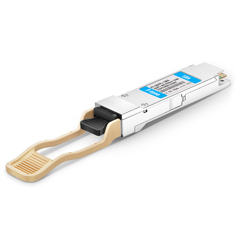
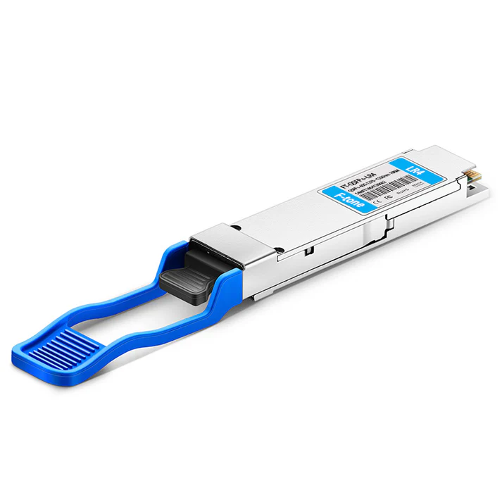
40Gbps QSFP+ Transceiver, Single Mode, 10km Reach
FTCQ-4X-CWDM4-10
Product Features
- 4 CWDM lanes MUX/DEMUX design
- Transmission data rate up to 11.3Gbps per channel
- SMF LC duplex connector
- Hot Pluggable QSFP+ form factor
- 1310nm DFB laser and PIN photodiode ,Up to 10km transmission
- Compatible with RoHS
- Single +3.3V power supply
- Real Time Digital Diagnostic Monitoring
- Compliant with QSFP+ MSA and IEEE 802.3ba 40GBASE-LR4 standard
- Low power consumption
- 2-wire serial interface for digital diagnostic
- Built-in laser safety compliance
- EMC compliant
- Operating case temperature: 0 to +70°C
Applications
- 40GBASE-LR4 Ethernet
- Switch, router and HBAs
- Data Center Interconnect
- Infiniband QDR
- 40G Campus Link
- Metro Access Network
- Storage Area Network (SAN)
Description
The QSFP+ LR4 transceivers are high performance, cost effective modules supporting data rate of 40Gbps and 10km transmission distance with SMF.
The transceiver consists of three sections: 4 inputs channels (ch) of 10Gb/s electrical data to 4 CWDM optical signals, and multiplexes them into a single channel for 40Gb/s optical transmission; on the receiver side, the module optically de-multiplexes a 40Gb/s input into 4 CWDM channels signals, and converts them to 4 channel output electrical data; and MCU control unit. All modules satisfy class I laser safety requirements.
The transceivers are compatible with 40GBASE-LR4 of IEEE802.3ba standard and SFF-8436 specification.
Absolute Maximum Ratings
|
Parameter |
Symbol |
Min |
Max |
Unit |
|
Supply Voltage |
Vcc |
-0.5 |
4.5 |
V |
|
Storage Temperature |
Ts |
-40 |
+85 |
°C |
|
Operating Humidity |
– |
5 |
85 |
% |
Recommended Operating Conditions
|
Parameter |
Symbol |
Min |
Typical |
Max |
Unit |
|
Operating Case Temperature |
Tc |
0 |
+70 |
°C |
|
|
Power Supply Voltage |
Vcc |
3.135 |
3.30 |
3.465 |
V |
|
Power Dissipation |
Pm |
3.5 |
W |
||
|
Data Rate |
10.3125 |
11.3 |
Gbps |
Optical and Electrical Characteristics
|
Parameter |
Symbol |
Min |
Typical |
Max |
Unit |
Notes |
|
|
Transmitter |
|||||||
|
Centre Wavelength |
L0 |
1264.5 |
1271 |
1277.5 |
nm |
||
|
L1 |
1284.5 |
1291 |
1297.5 |
nm |
|||
|
L2 |
1304.5 |
1311 |
1317.5 |
nm |
|||
|
L3 |
1324.5 |
1331 |
1337.5 |
nm |
|||
|
-20dB Spectral Width |
Δλ |
1 |
nm |
||||
|
Side-mode Suppression Ratio |
SMSR |
30 |
– |
dB |
|||
|
Total Average Launch Power |
PT |
8.3 |
dBm |
||||
|
Average launch power, each lane |
Pout |
-7 |
2.3 |
dBm |
|||
|
Extinction Ratio |
ER |
3.5 |
dB |
||||
|
Average launch power of OFF transmitter,each lane |
Poff |
-30 |
dBm |
||||
|
Relative Intensity Noise |
Rin |
-128 |
dB/Hz |
12dB reflection |
|||
|
Transmitter Reflectance |
RT |
-12 |
dB |
||||
|
Data Input Swing Differential |
VIN |
190 |
700 |
mV |
|||
|
Input Differential Impedance |
ZIN |
90 |
100 |
110 |
Ω |
||
|
Receiver |
|||||||
|
Centre Wavelength |
L0 |
1264.5 |
1271 |
1277.5 |
nm |
||
|
L1 |
1284.5 |
1291 |
1297.5 |
nm |
|||
|
L2 |
1304.5 |
1311 |
1317.5 |
nm |
|||
|
L3 |
1324.5 |
1331 |
1337.5 |
nm |
|||
|
Damage threshold |
THd |
3.3 |
dBm |
||||
|
Average power at receiver input,each lane |
-13.7 |
2.3 |
dBm |
||||
|
Receiver sensitivity (OMA), each lane |
-11.5 |
dBm |
|||||
|
LOS De-Assert |
LOSD |
-15 |
dBm |
||||
|
LOS Assert |
LOSA |
-30 |
dBm |
||||
|
LOS Hysteresis |
0.5 |
dB |
|||||
|
Receive Electrical 3 dB upper Cutoff Frequency, each Lane |
Fc |
11.3 |
GHz |
||||
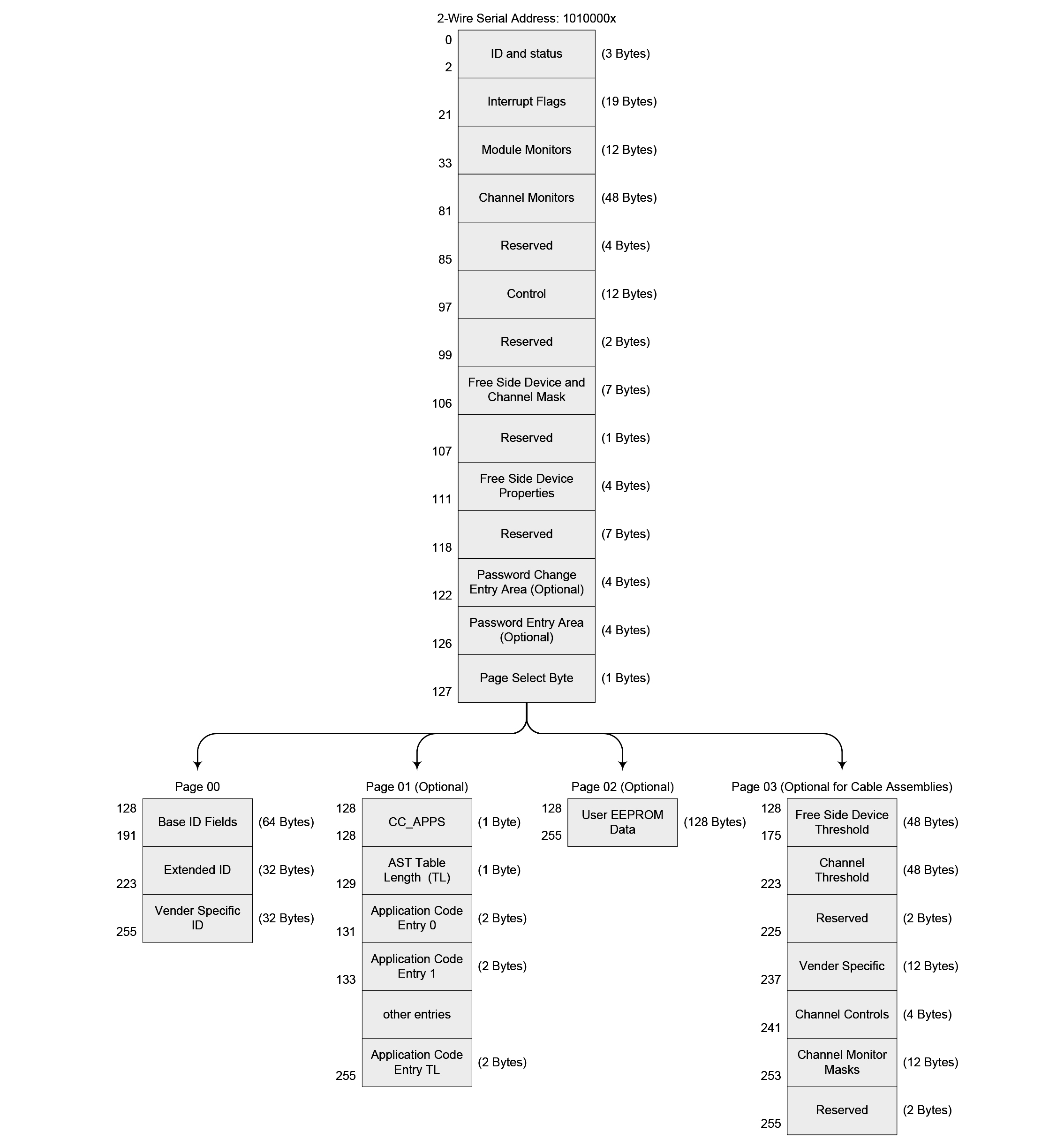
Digital Diagnostic Memory Map
The transceivers provide serial ID memory contents and diagnostic information about the present operating conditions by the 2-wire serial interface (SCL, SDA).
The digital diagnostic memory map specific data field defines as following.
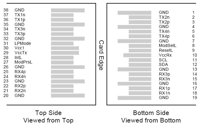
Pin Descriptions
|
PIN |
Logic |
Symbol |
Name/Description |
Note |
|---|---|---|---|---|
|
1 |
|
GND |
Ground |
1 |
|
2 |
CML-I |
Tx2n |
Transmitter Inverted Data Input |
|
|
3 |
CML-I |
Tx2p |
Transmitter Non-Inverted Data Input |
|
|
4 |
|
GND |
Ground |
1 |
|
5 |
CML-I |
Tx4n |
Transmitter Inverted Data Input |
|
|
6 |
CML-I |
Tx4p |
Transmitter Non-Inverted Data Input |
|
|
7 |
|
GND |
Ground |
1 |
|
8 |
LVTLL-I |
ModSelL |
Module Select |
|
|
9 |
LVTLL-I |
ResetL |
Module Reset |
|
|
10 |
|
VccRx |
﹢3.3V Power Supply Receiver |
2 |
|
11 |
LVCMOS-I/O |
SCL |
2-Wire Serial Interface Clock |
|
|
12 |
LVCMOS-I/O |
SDA |
2-Wire Serial Interface Data |
|
|
13 |
|
GND |
Ground |
|
|
14 |
CML-O |
Rx3p |
Receiver Non-Inverted Data Output |
|
|
15 |
CML-O |
Rx3n |
Receiver Inverted Data Output |
|
|
16 |
|
GND |
Ground |
1 |
|
17 |
CML-O |
Rx1p |
Receiver Non-Inverted Data Output |
|
|
18 |
CML-O |
Rx1n |
Receiver Inverted Data Output |
|
|
19 |
|
GND |
Ground |
1 |
|
20 |
|
GND |
Ground |
1 |
|
21 |
CML-O |
Rx2n |
Receiver Inverted Data Output |
|
|
22 |
CML-O |
Rx2p |
Receiver Non-Inverted Data Output |
|
|
23 |
|
GND |
Ground |
1 |
|
24 |
CML-O |
Rx4n |
Receiver Inverted Data Output |
1 |
|
25 |
CML-O |
Rx4p |
Receiver Non-Inverted Data Output |
|
|
26 |
|
GND |
Ground |
1 |
|
27 |
LVTTL-O |
ModPrsL |
Module Present |
|
|
28 |
LVTTL-O |
IntL |
Interrupt |
|
|
29 |
|
VccTx |
+3.3 V Power Supply transmitter |
2 |
|
30 |
|
Vcc1 |
+3.3 V Power Supply |
2 |
|
31 |
LVTTL-I |
LPMode |
Low Power Mode |
|
|
32 |
|
GND |
Ground |
1 |
|
33 |
CML-I |
Tx3p |
Transmitter Non-Inverted Data Input |
|
|
34 |
CML-I |
Tx3n |
Transmitter Inverted Data Input |
|
|
35 |
|
GND |
Ground |
1 |
|
36 |
CML-I |
Tx1p |
Transmitter Non-Inverted Data Input |
|
|
37 |
CML-I |
Tx1n |
Transmitter Inverted Data Input |
|
|
38 |
|
GND |
Ground |
1 |
Notes:
1. GND is the symbol for signal and supply (power) common for QSFP modules. All are common within the QSFP module and all module voltages are referenced to this potential unless otherwise noted. Connect these directly to the host board signal common ground plane.
2. VccRx, Vcc1 and VccTx are the receiver and transmitter power suppliers and shall be applied concurrently. Recommended host board power supply filtering is shown below. Vcc Rx, Vcc1 and Vcc Tx may be internally connected within the QSFP transceiver module in any combination. The connector pins are each rated for a maximum current of 500mA.
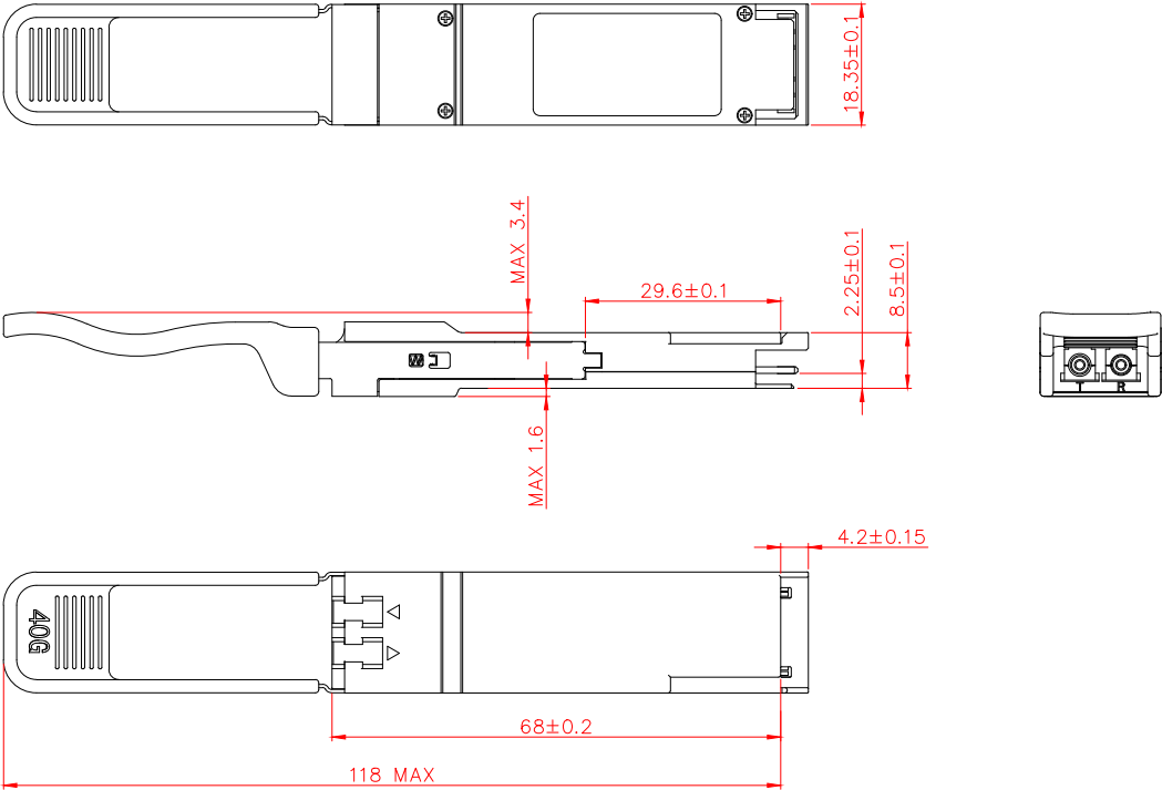
Mechanical Dimensions
Ordering information
|
Part Number |