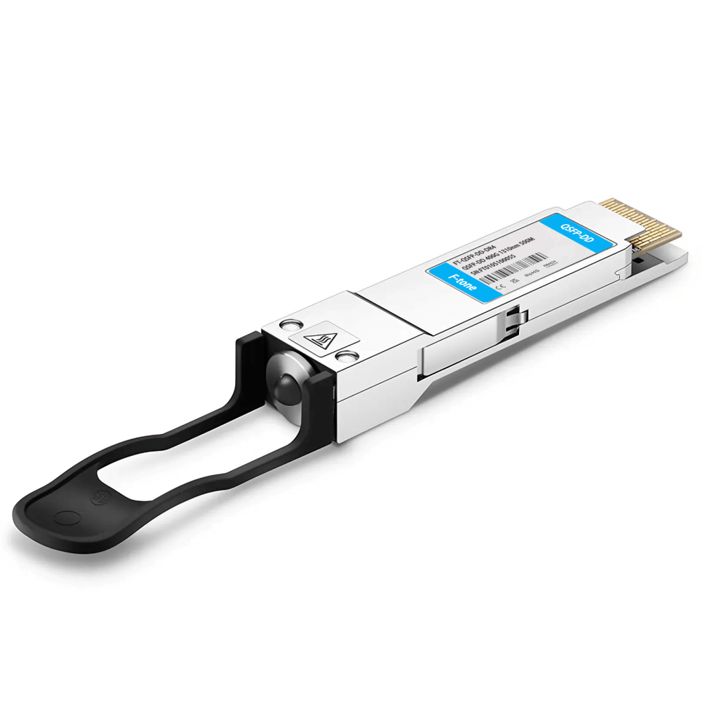
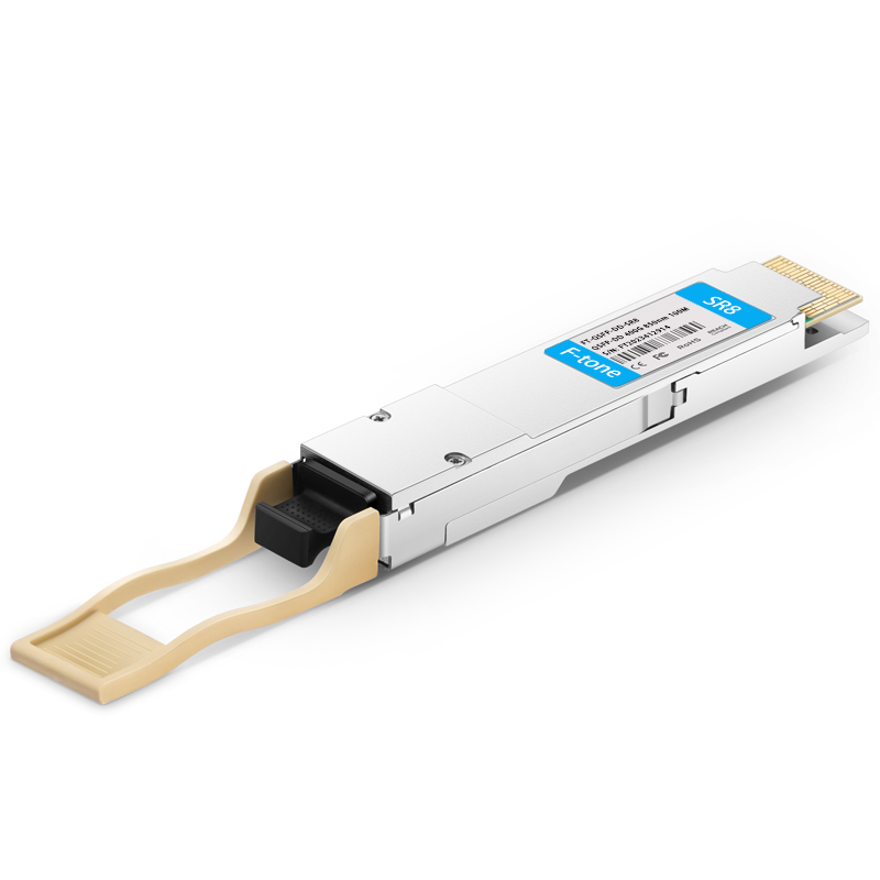
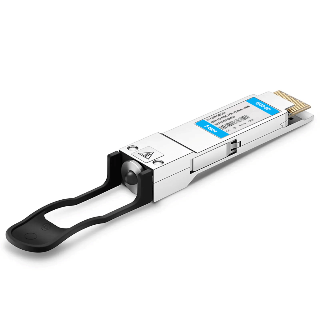
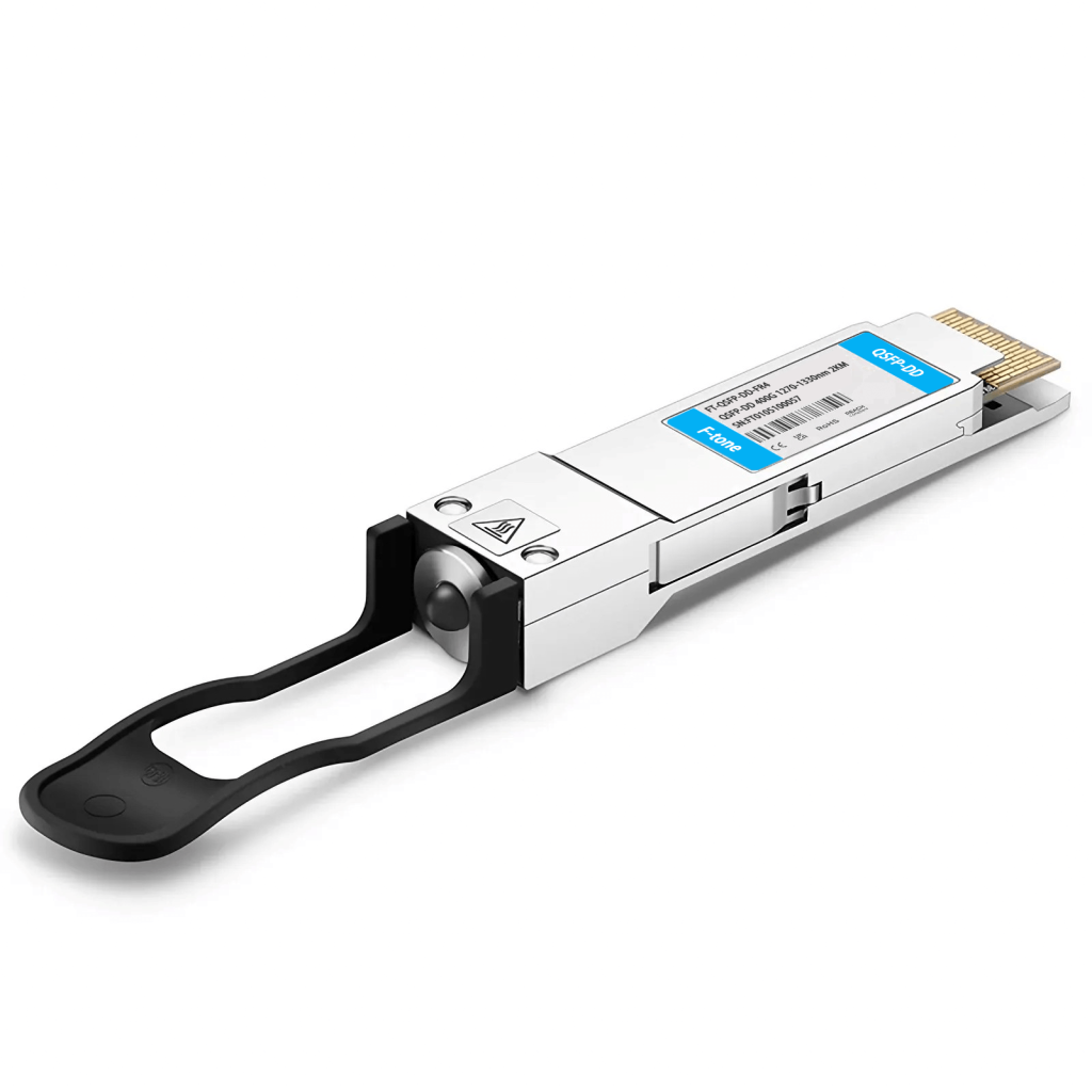
400G QSFP-DD XPSM8 20km Optical Transceiver Module
FTQD-4H-XPSM8-20KM
Features
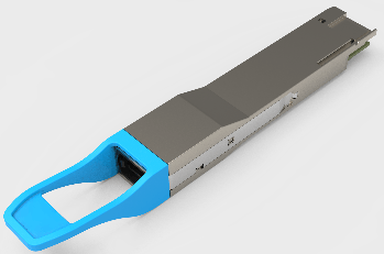 8 channels full-duplex transceiver modules
 - Transmission data rate up to 53Gbps per channel
- 8x53Gbps PAM4 transmitter and PAM4 receiver
- 8 channels1310nm cooled EML
- 8 channels PIN photo detector array
- Internal CDR circuits on both receiver and transmitter channels
- Power consumption <11W
- Hot Pluggable QSFP DD form factor and Compliant with CMIS 4.0
- Maximum link length of 20km G.652 SMF with KP-FEC
- MPO16 APC connector receptacle
- Built-in digital diagnostic functions
- Operating case temperature 0°C to +70°C
- 3.3V power supply voltage
- RoHS compliant(lead free)
Applications
- IEEE 802.3bs 200GBASE-DR4
- 2x200G Ethernet Applications
Description
The F-tone Networks FTQD-4H-XPSM8-20KM is an Eight-Channel, Pluggable, Parallel, Fiber-Optic QSFP Double Density for 2×200 Gigabit Ethernet Applications. This transceiver is a high performance module for multi-lane data communication and interconnection applications. It integrates eight data lanes in each direction with 8×26.5625GBd. Each lane can operate at 53.125Gbps up to 20km using G.652 SMF with KP-FEC. These modules are designed to operate over singlemode fiber systems using a nominal wavelength of 1310nm. The electrical interface 400GAUI-8 uses a 76 contact edge type connector. The optical interface uses a MPO16/MTP16 APC connector . The Common Management Interface Specification (CMIS) for QSFP DD modules, This module incorporates F-tone Networks proven circuit and EML technology to provide reliable long life, high performance, and consistent service.
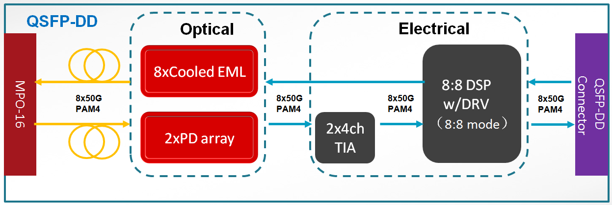
Figure1. Module Block Diagram
FTQD-4H-XPSM8-20KM is one kind of parallel transceiver. EML and PIN array package are key technique, through I2C system can contact with module.
Absolute Maximum Ratings
|
Parameter |
Symbol |
Min |
Max |
Unit |
|
Supply Voltage |
Vcc |
-0.3 |
3.6 |
V |
|
Input Voltage |
Vin |
-0.3 |
Vcc+0.3 |
V |
|
Storage Temperature |
Tst |
-20 |
85 |
ºC |
|
Case Operating Temperature |
Top |
0 |
70 |
ºC |
|
Humidity(non-condensing) |
Rh |
5 |
95 |
% |
Recommended Operating Conditions
|
Parameter |
Symbol |
Min |
Typical |
Max |
Unit |
|
Supply Voltage |
Vcc |
3.13 |
3.3 |
3.47 |
V |
|
Operating Case temperature |
Tca |
0 |
70 |
ºC |
|
|
Data Rate Per Lane |
fd |
26.5625 |
GBd |
||
|
Humidity |
Rh |
5 |
85 |
% |
|
|
Power Dissipation |
Pm |
11 |
W |
Electrical Specifications
|
Parameter |
Symbol |
Min |
Typical |
Max |
Unit |
|
Differential input impedance |
Zin |
90 |
100 |
110 |
ohm |
|
Differential Output impedance |
Zout |
90 |
100 |
110 |
ohm |
|
Differential input voltage amplitude |
ΔVin |
900 |
1200 |
mVp-p |
|
|
Differential output voltage amplitude |
ΔVout |
1100 |
mVp-p |
||
|
Skew |
Sw |
300 |
ps |
||
|
Bit Error Rate |
BER |
2.4E-4 |
– |
||
|
Near-end Eye Width at 10^-6 probability(EW6) |
0.265 |
UI |
|||
|
Near-end Eye Height at 10^-6 probability(EH6) |
70 |
mV |
|||
|
Far-end Eye Width at 10^-6 probability(EW6) |
0.20 |
UI |
|||
|
Far-end Eye Height at 10^-6 probability(EH6) |
30 |
mV |
|||
|
Near-end Eye Linearity |
0.85 |
– |
Note:
- BER=2.4E-4; PRBS31Q@26.5625GBd. Pre-FEC
2. Differential input voltage amplitude is measured between TxnP and TxnN.
3. Differential output voltage amplitude is measured between RxnP and RxnN.
Optical Characteristics
Table 3 – Optical Characteristics
|
Parameter |
Symbol |
Min |
Typical |
Max |
Unit |
Notes |
|
Transmitter |
||||||
|
Centre Wavelength |
λc |
1304.5 |
— |
1317.5 |
nm |
– |
|
Side-mode suppression ratio |
SMSR |
30 |
– |
— |
dB |
– |
|
Average launch power, each lane |
Pout |
-4.1 |
– |
4 |
dBm |
– |
|
Optical Modulation Amplitude (OMAouter), each lane |
OMA |
-2 |
3.8 |
dBm |
– |
|
|
Transmitter and dispersion eye closure(TDEC),each lane |
TDEC |
3.4 |
dB |
|||
|
Extinction Ratio |
ER |
3.5 |
– |
– |
dB |
– |
|
Average launch power of OFF transmitter, each lane |
-30 |
dB |
– |
|||
|
Receiver |
||||||
|
Centre Wavelength |
λc |
1304.5 |
— |
1317.5 |
nm |
– |
|
Receiver Sensitivity in OMAouter |
RXsen |
-10 |
-9 |
dBm |
1 |
|
|
Average power at receiver , each lane input, each lane |
Pin |
-9 |
4 |
dBm |
– |
|
|
Receiver Reflectance |
-12 |
dB |
– |
|||
|
LOS Assert |
-13.5 |
dBm |
– |
|||
|
LOS De-Assert – OMA |
-12 |
dBm |
– |
|||
|
LOS Hysteresis |
0.5 |
dB |
– |
|||
Note:
- Measured with conformance test signal at TP3 for BER = 2.4E-4 Pre-FEC
Pin Description
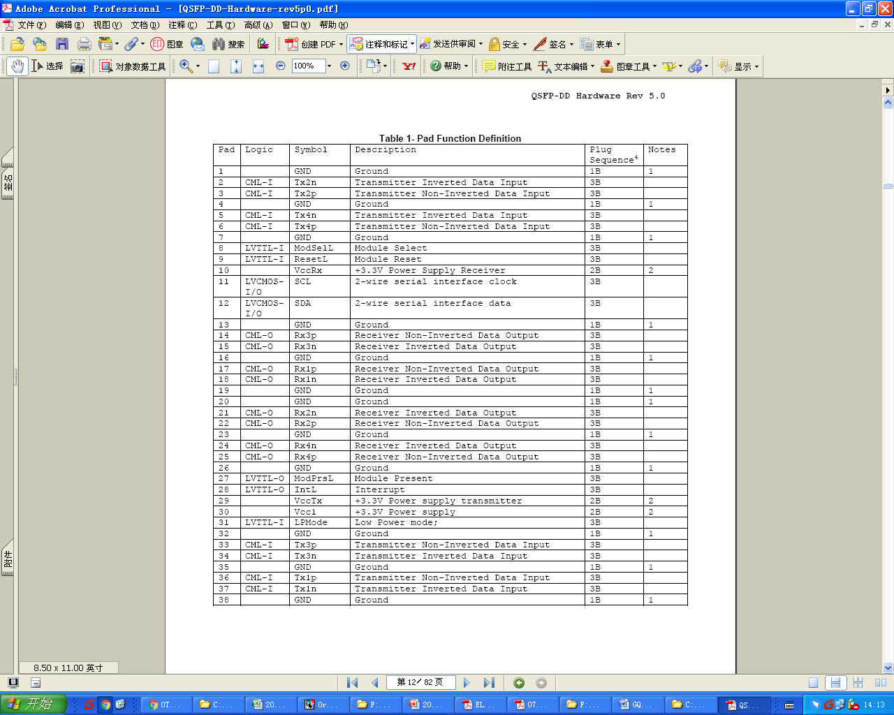
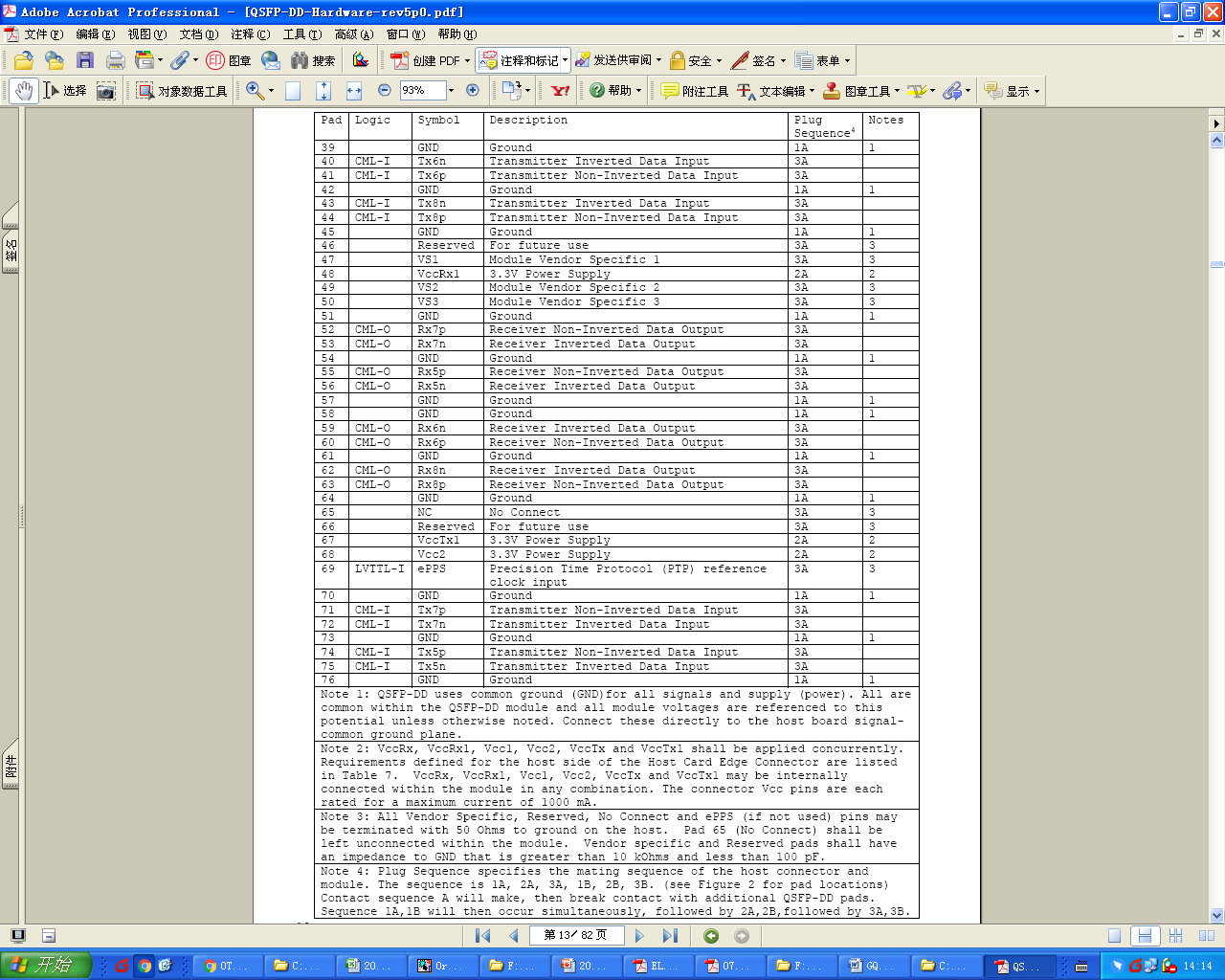
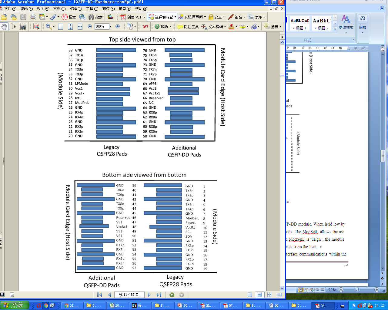
Figure2. Electrical Pin-out Details
ModSelL Pin
The ModSelL is an input signal that shall be pulled to Vcc in the QSFP-DD module. When held low by the host, the module responds to 2-wire serial communication commands. The ModSelL allows the use of multiple QSFP-DD modules on a single 2-wire interface bus. When ModSelL is “High”, the module shall not respond to or acknowledge any 2-wire interface communication from the host.
In order to avoid conflicts, the host system shall not attempt 2-wire interface communications within the ModSelL de-assert time after any QSFP-DD modules are deselected. Similarly, the host must wait at least for the period of the ModSelL assert time before communicating with the newly selected module. The assertion and de-asserting periods of different modules may overlap as long as the above timing requirements are met.
ResetL Pin
The ResetL signal shall be pulled to Vcc in the module. A low level on the ResetL signal for longer than the minimum pulse length (t_Reset_init) initiates a complete module reset, returning all user module settings to their default state.
LPMode Pin
LPMode is an input signal. The LPMode signal shall be pulled up to Vcc in the QSFP-DD module. LPMode is used in the control of the module power mode. See CMIS Section 6.3.1.3.
ModPrsL Pin
ModPrsL shall be pulled up to Vcc Host on the host board and pulled low in the module. The ModPrsL is asserted “Low” when the module is inserted. The ModPrsL is deasserted “High” when the module is physically absent from the host connector due to the pull-up resistor on the host board.
IntL Pin
IntL is an output signal. The IntL signal is an open collector output and shall be pulled to Vcc Host on the host board. When the IntL signal is asserted Low it indicates a change in module state, a possible module operational fault or a status critical to the host system. The host identifies the source of the interrupt using the 2-wire serial interface. The IntL signal is deasserted “High” after all set interrupt flags are read.
Power Supply Filtering
The host board should use the power supply filtering shown in Figure3.
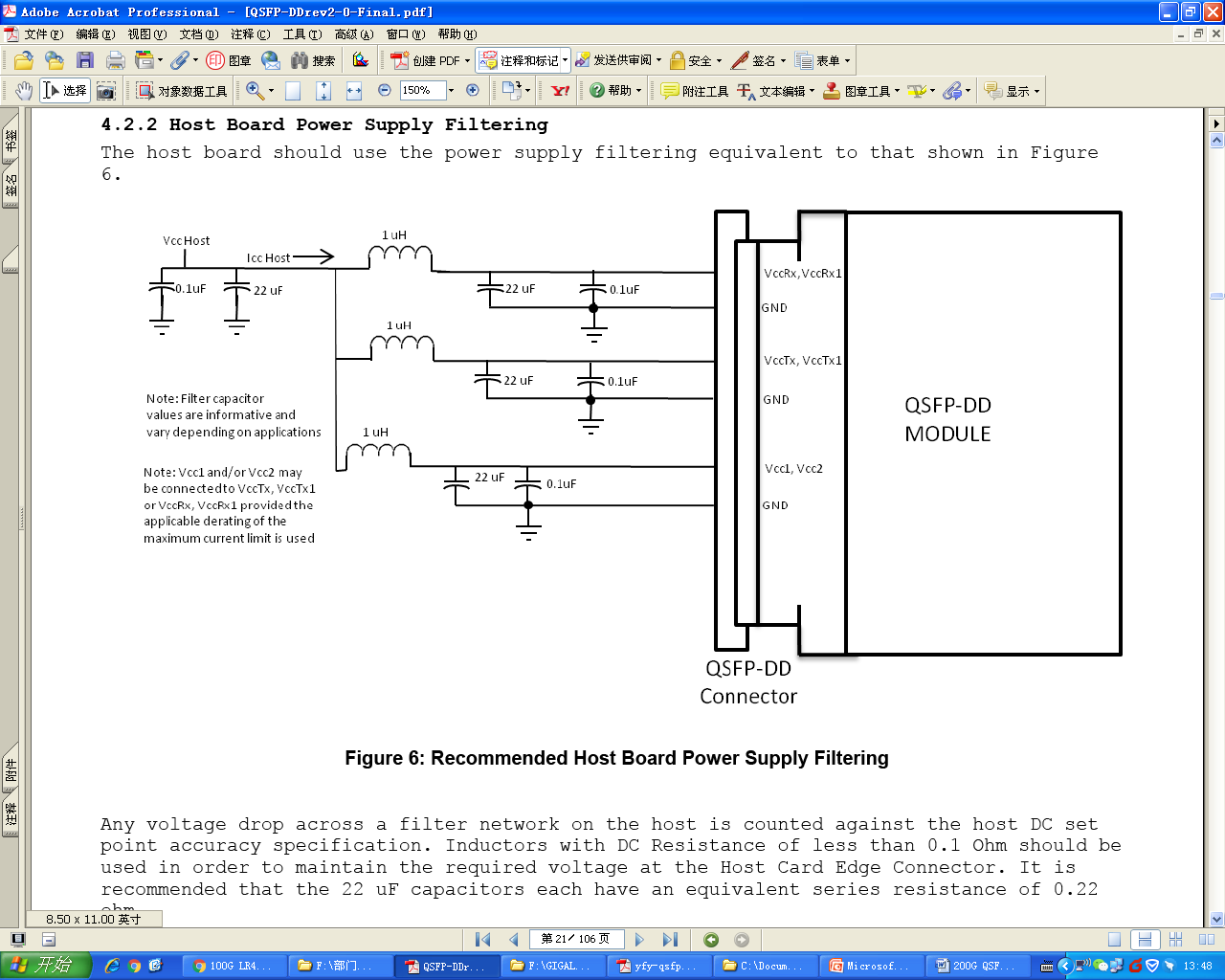
Figure3. Host Board Power Supply Filtering
Optical Interface Lanes and Assignment
The optical interface port is a male MPO16(MTP16) APC connector.
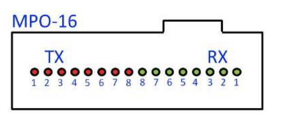
Figure 4. Optical Receptacle and Channel Orientation
DIAGNOSTIC MONITORING INTERFACE
Digital diagnostics monitoring function is available on all F-tone Networks QSFP DD products. A 2-wire serial interface provides user to contact with module.
Memory Structure and Mapping
This limits the management memory that can be directly accessed by the host to 256 bytes, which is divided in Lower Memory (addresses 00h through 7Fh) and Upper Memory (addresses 80h through FFh).
A larger addressable management memory is required for all but the most basic modules. This is supported by a structure of 128-byte pages, together with a mechanism for dynamically mapping any of the 128-byte pages from a larger internal management memory space into Upper Memory the host addressable space.