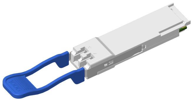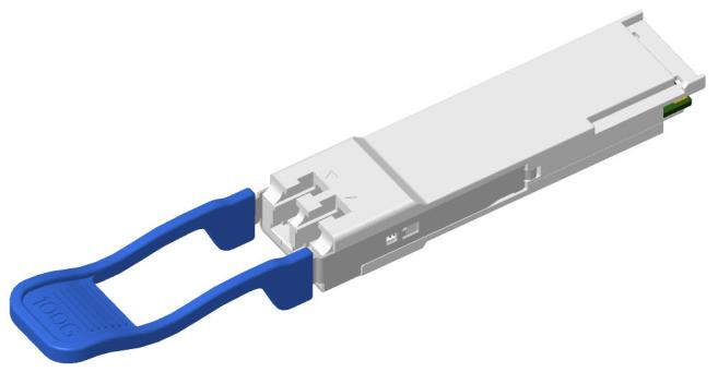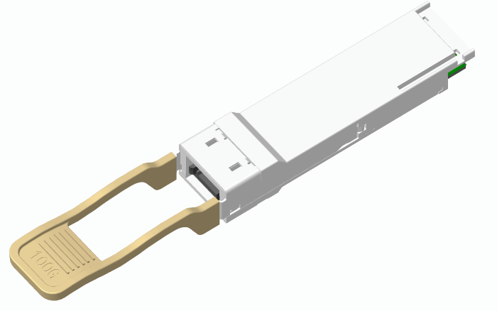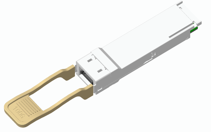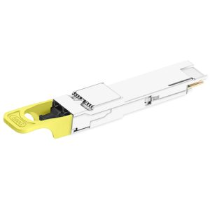
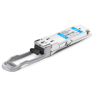
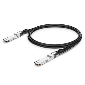

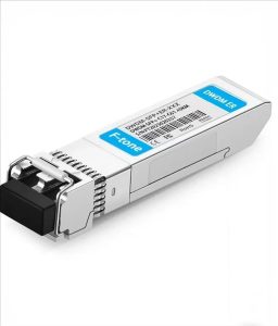
F-tone Networks 的 FTQ2-HG-ZRx(x = R/S,t = 1/4)是一款 QSFP28 封装的数字相干光(DCO)模块,面向边缘网络应用,支持最远 120km 的 100G 传输(色散受限,可选扩展至 300km)。在主机侧,模块可承载 IEEE 100GE 以太网或 ITU-T OTN OTU4 信号。线路侧相干接口指标对齐 IEEE Std. 802.3-2022 100GBASE-ZR 与 ITU-T G.698.2 DW50U-8A2(C)F / DW100U-8A2(C)F,采用 27.95GBd 双偏振差分 QPSK 调制格式。
模块提供商业级温度(0℃ ~ 70℃,C-temp)与工业级温度(-40℃ ~ 85℃,I-temp)两个版本,功耗低于 6.0W。本振激光器全 C 波段可调,可选配 Flextune™ 自动波长调谐功能。
模块符合 QSFP+ 28 Gb/s 4X Pluggable Transceiver Solution(QSFP28)规范及其引用规范,并按 Application Note AN-2038 满足 RoHS 要求。
产品特性 / Features
- 热插拔 QSFP28 封装
- 主机接口兼容 IEEE 100G 以太网(CAUI-4)或 ITU-T 100G OTN(OTL4.4)
- 100G 光接口采用 DP-DQPSK 调制与 Staircase FEC,符合 IEEE Std. 802.3-2022 100GBASE-ZR 或 ITU-T G.709.2
- 传输距离:无放大最远 80km(损耗受限);带放大最远 120km(色散受限,可选扩展至 300km)
- 全 C 波段可调,50GHz 或 100GHz 栅格,可选 Flextune™ 自动波长调谐
- 外壳工作温度 0℃ ~ 70℃(C-temp)或 -40℃ ~ 85℃(I-temp)
- 功耗 < 5.5W(C-temp)或 < 6.0W(I-temp)
- 支持远程数字诊断监控(DDM)
应用领域 / Applications
- 接入与汇聚网络(Access and aggregation networks)
- 有线电视网络(Cable TV networks)
- 无线前传与中传(Wireless front-haul & mid-haul)
引脚定义 / Pin Definitions
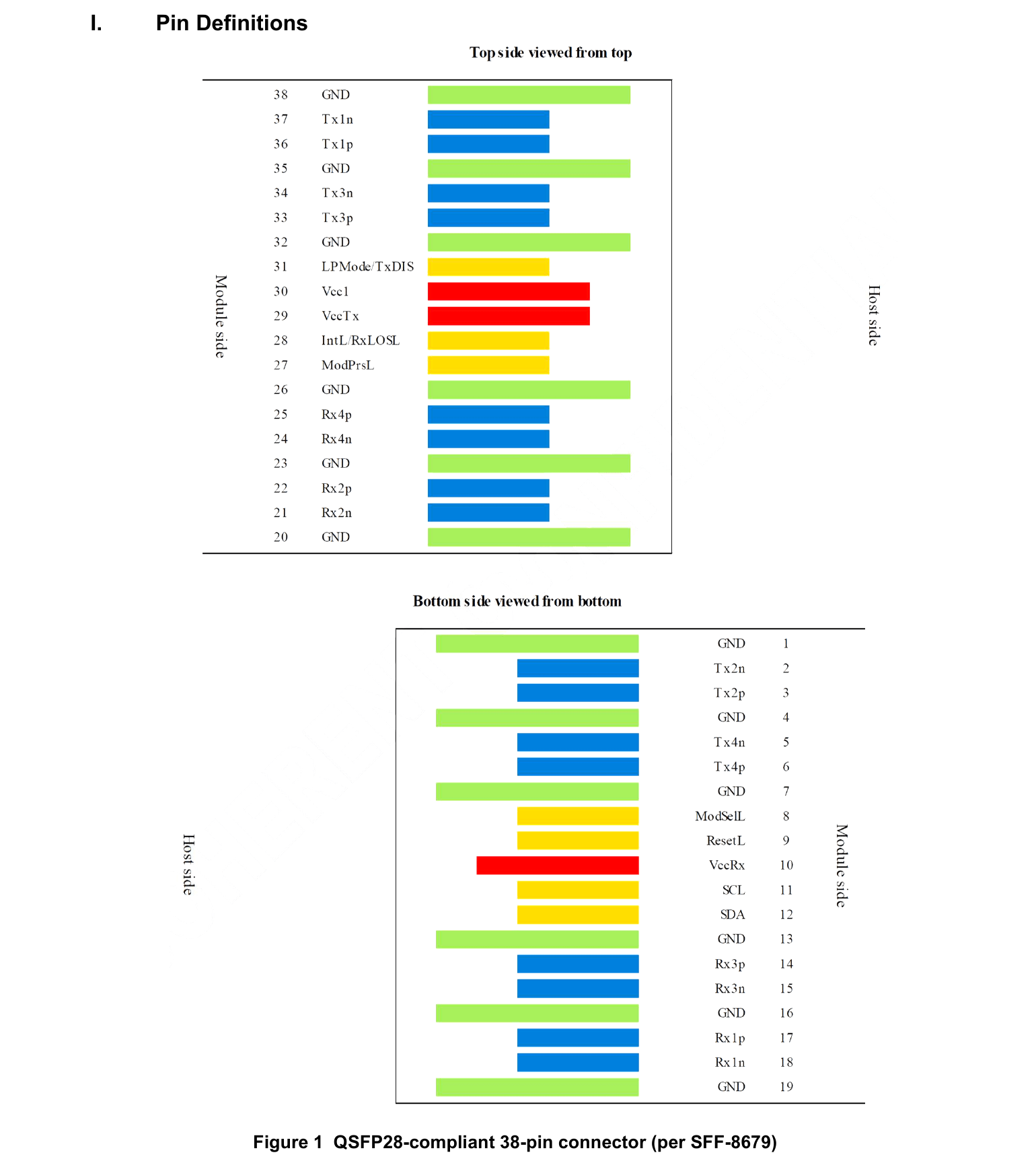
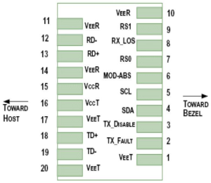
Figure 1 符合 SFF-8679 的 QSFP28 38-pin 连接器引脚定义
| Pin | Logic | Symbol | Description | Plug Sequence | Notes |
|---|---|---|---|---|---|
| 1 | GND | Ground | 1 | 1 | |
| 2 | CML-I | Tx2n | Transmitter inverted data input | 3 | |
| 3 | CML-I | Tx2p | Transmitter non-inverted data input | 3 | |
| 4 | GND | Ground | 1 | 1 | |
| 5 | CML-I | Tx4n | Transmitter inverted data input | 3 | |
| 6 | CML-I | Tx4p | Transmitter non-inverted data input | 3 | |
| 7 | GND | Ground | 1 | 1 | |
| 8 | LVTTL-I | ModSelL | Module select | 3 | |
| 9 | LVTTL-I | ResetL | Module reset | 3 | |
| 10 | VccRx | +3.3V power supply receiver | 2 | 2 | |
| 11 | LVCMOS-I/O | SCL | 2-wire serial interface clock | 3 | |
| 12 | LVCMOS-I/O | SDA | 2-wire serial interface data | 3 | |
| 13 | GND | Ground | 1 | 1 | |
| 14 | CML-O | Rx3p | Receiver non-inverted data output | 3 | |
| 15 | CML-O | Rx3n | Receiver inverted data output | 3 | |
| 16 | GND | Ground | 1 | 1 | |
| 17 | CML-O | Rx1p | Receiver non-inverted data output | 3 | |
| 18 | CML-O | Rx1n | Receiver inverted data output | 3 | |
| 19 | GND | Ground | 1 | 1 | |
| 20 | GND | Ground | 1 | 1 | |
| 21 | CML-O | Rx2n | Receiver inverted data output | 3 | |
| 22 | CML-O | Rx2p | Receiver non-inverted data output | 3 | |
| 23 | GND | Ground | 1 | 1 | |
| 24 | CML-O | Rx4n | Receiver inverted data output | 3 | |
| 25 | CML-O | Rx4p | Receiver non-inverted data output | 3 | |
| 26 | GND | Ground | 1 | 1 | |
| 27 | LVTTL-O | ModPrsL | Module present | 3 | |
| 28 | LVTTL-O | IntL/RxLOSL | Interrupt;可通过管理接口(CMIS / SFF-8636)配置为 RxLOSL | 3 | |
| 29 | VccTx | +3.3V power supply transmitter | 2 | 2 | |
| 30 | Vcc1 | +3.3V power supply | 2 | 2 | |
| 31 | LVTTL-I | LPMode/TxDIS | Low power mode;可通过管理接口(CMIS / SFF-8636)配置为 TxDis | 3 | |
| 32 | GND | Ground | 1 | 1 | |
| 33 | CML-I | Tx3p | Transmitter non-inverted data input | 3 | |
| 34 | CML-I | Tx3n | Transmitter inverted data input | 3 | |
| 35 | GND | Ground | 1 | 1 | |
| 36 | CML-I | Tx1p | Transmitter non-inverted data input | 3 | |
| 37 | CML-I | Tx1n | Transmitter inverted data input | 3 | |
| 38 | GND | Ground | 1 | 1 |
1. GND 为模块信号与电源公共地,模块内部全部连通,除特别说明外所有电压均以此为参考,应直接连至主机板信号公共地平面。
2. VccRx、Vcc1、VccTx 同时供电,模块内部可任意组合连通。
3. Plug Sequence 表示主机连接器与模块的插合顺序,为 1、2、3(焊盘位置见图 1)。
绝对最大额定值 / Absolute Maximum Ratings
超出绝对最大额定值的应力可能造成器件永久损坏。以下仅为绝对应力额定值,不表示器件在这些条件下或超出规格书工作条件的任何其他条件下可正常工作。长时间暴露于绝对最大额定值会降低器件可靠性。
| Parameter | Conditions | Symbol | Min | Typ | Max | Unit |
|---|---|---|---|---|---|---|
| DC supply voltage | VCC | -0.3 | 3.6 | V | ||
| Low speed I/O voltages | -0.3 | 3.6 | V | |||
| Storage temperature | TS | -40 | 85 | ℃ | ||
| Case operating temperature | Central office applications (C-temp) | TOP | -5 | 75 | ℃ | |
| Case operating temperature | Outside plant applications (I-temp) | TOP | -40 | 85 | ℃ | |
| Relative humidity | Non-condensing | RH | 5 | 95 | % | |
| Rx input power | PRx,in | 10 | dBm | |||
| ESD damage threshold | Human body model (HBM),DC pins | 2000 | V | |||
| ESD damage threshold | Human body model (HBM),RF pins | 1000 | V |
注意:使用非本规格书规定的控制、调整或操作程序,可能导致有害辐射暴露。
环境规格 / Environmental Specifications
| Parameter | Conditions | Symbol | Min | Typ | Max | Unit |
|---|---|---|---|---|---|---|
| Storage temperature | TS | -40 | 85 | ℃ | ||
| Case operating temperature | Central office appl. (C-temp),长期 | TOP | 0 | 70 | ℃ | |
| Case operating temperature | Central office appl. (C-temp),短期 < 96h | TOP | -5 | 75 | ℃ | |
| Case operating temperature | Outside plant appl. (I-temp),长期 | TOP | -20 | 85 | ℃ | |
| Case operating temperature | Outside plant appl. (I-temp),启动 | TOP | -40 | 85 | ℃ | |
| Relative humidity | Non-condensing | RH | 5 | 85 | % |
1. 冷启动期间无需满足光学性能指标,但模块应能上电并响应命令。
数据通道 / Data Path
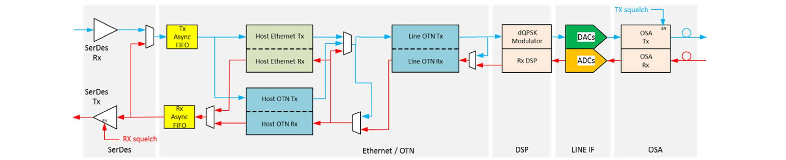
Figure 2 FTQ2-HG-ZRx(x = R/S,t = 1/4)模块数据通道高层框图
A. 主机接口模式 / Host Interface Modes
| Host Interface ID | Host Interface Description | Modulation | Forward Error Correction | Nominal Symbol Rate (GBd) | Supported Line Interface IDs |
|---|---|---|---|---|---|
| 65 | CAUI-4 C2M without FEC | NRZ | None | 25.78125 | 68, 192, 193 |
| 66 | CAUI-4 C2M with RS(528,514) FEC | NRZ | RS(528,514) | 25.78125 | 68, 192, 193 |
| 57 | OTL4.4 (ITU-T G.709 / Y.1331 G.Sup58) | NRZ | RS(255,239) | 27.9525 | 192, 193 |
B. 线路接口模式 / Line Interface Modes
| Line Interface ID | Line Interface Description | Modulation | Forward Error Correction | Nominal Symbol Rate (GBd) | Spectral Shaping |
|---|---|---|---|---|---|
| 68 | 100GBASE-ZR (Clause 154) | DP-DQPSK | Staircase (SC) | 27.9525 | None |
| 192 | OTU4 Long Reach | DP-DQPSK | Staircase (SC) | 27.9525 | |
| 193 | OTU4 Short Reach | DP-DQPSK | RS(255,239) | 27.9525 | None |
C. 数据通道参数 / Data Path Parameters
| Parameter | Conditions | Min | Typ | Max | Unit |
|---|---|---|---|---|---|
| End-to-end module transit delay | 100G DQPSK SC line mode | 24 | μs | ||
| End-to-end module transit delay | 100G DQPSK RS line mode | 5 | μs | ||
| Delay variation | 100GE CAUI-4 host mode | -10 | 10 | ns | |
| Delay variation | OTU4 OTL4.4 host mode | -6 | 6 | ns |
1. 时延抖动为两只 FTQ2-HG-ZRx 模块在长时间(含冷重启)内的最大偏差,测量时使用 0.1Hz 带宽低通滤波,用于支持 IEEE 1588-2019 精确时间协议报文的透明传输(Class C 运行)。
电气特性 / Electrical Characteristics
A. 电源与低速 I/O / Power & Low Speed I/O
| Parameter | Conditions | Symbol | Min | Typ | Max | Unit |
|---|---|---|---|---|---|---|
| Power supply voltages | 含 100kHz 以下纹波、跌落与噪声 | 3.135 | 3.300 | 3.465 | V | |
| Host RMS noise output | 10Hz – 10MHz | 25 | mV | |||
| Module RMS noise output | 10Hz – 10MHz | 15 | mV | |||
| Module supply noise tolerance | 10Hz – 10MHz,峰峰值 | PSNRmod | 66 | mV | ||
| Module inrush | 瞬时峰值持续时间 | Tip | 50 | μs | ||
| Module inrush | 初始化时间 | Tinit | 500 | ms | ||
| Power dissipation(低功耗模式) | Plp | 1.5 | W | |||
| Power supply current(低功耗模式) | 瞬时峰值电流 | ICC,ip,lp | 600 | mA | ||
| Power supply current(低功耗模式) | 持续峰值电流 | ICC,sp,lp | 495 | mA | ||
| Power supply current(低功耗模式) | 稳态电流 | ICC,lp | 478 | mA | ||
| Power dissipation(高功耗模式,C-temp) | Php | 5.5 | W | |||
| Power supply current(高功耗模式,C-temp) | 瞬时峰值电流 | ICC,ip,hp | 2200 | mA | ||
| Power supply current(高功耗模式,C-temp) | 持续峰值电流 | ICC,sp,hp | 1815 | mA | ||
| Power supply current(高功耗模式,C-temp) | 稳态电流 | ICC,hp | 1754 | mA | ||
| Power dissipation(高功耗模式,I-temp) | Php | 6.0 | W | |||
| Power supply current(高功耗模式,I-temp) | 瞬时峰值电流 | ICC,ip,hp | 2400 | mA | ||
| Power supply current(高功耗模式,I-temp) | 持续峰值电流 | ICC,sp,hp | 1980 | mA | ||
| Power supply current(高功耗模式,I-temp) | 稳态电流 | ICC,hp | 1914 | mA | ||
| Clock frequency, SCL | Default | fSCL | 400 | kHz | ||
| Clock frequency, SCL | Fast mode+ | fSCL | 1000 | kHz | ||
| Output voltage, SCL and SDA | Output low | VOL | 0.0 | 0.4 | V | |
| Output voltage, SCL and SDA | Output high | VOH | VCC-0.5 | VCC+0.3 | V | |
| Input voltage, SCL and SDA | Input low | VIL | -0.3 | 0.63 | V | |
| Input voltage, SCL and SDA | Input high | VIH | 0.7×VCC | VCC+0.5 | V | |
| Capacitance for SCL and SDA I/O signal | Ci | 14 | pF | |||
| Total bus capacitive load for SCL and SDA | 400kHz 时钟,最大 3.0kΩ 上拉 | Cb | 100 | pF | ||
| Total bus capacitive load for SCL and SDA | 400kHz 时钟,最大 1.6kΩ 上拉 | Cb | 200 | pF | ||
| Input voltage / current,LPMode/TxDis、ResetL、ModSelL | Input voltage, low | VIL | -0.3 | 0.8 | V | |
| Input voltage / current,LPMode/TxDis、ResetL、ModSelL | Input voltage, high | VIH | 2.0 | VCC+0.3 | V | |
| Input voltage / current,LPMode/TxDis、ResetL、ModSelL | Input current,0V < Vin < VCC | Iin | -365 | 125 | μA | |
| Output voltage,ModPrsL、IntL/RxLOSL | Output low,IOL = 2mA | VOL | 0.0 | 0.4 | V | |
| Output voltage,ModPrsL、IntL/RxLOSL | Output high,10kΩ 上拉至主机 VCC | VOH | VCC-0.5 | VCC+0.3 | V |
1. 在所有供电电压下,模块功耗均保持在标称功率等级内。
2. 1000kHz 时钟速率请参阅 IEEE Std 802.3 图 6-4。
B. 高速数据 I/O / High Speed Data I/O
高速数据 I/O 各项指标按下列标准执行,本规格书不再单列数值;如需具体测试报告,请联系销售人员。
| 接口方向 | 参数项 | 依据标准 |
|---|---|---|
| Transmitter (module input) – CAUI-4 | Signaling rate per lane、Differential pk-pk input voltage tolerance、Differential input return loss、Differential to common mode input return loss、Differential termination mismatch、Module stressed input test、Single-ended voltage tolerance range、DC common mode voltage | IEEE Std 802.3,Annex 83E,Table 83E-7 |
| Transmitter (module input) – OTL4.4 | Overload differential voltage pk-pk、Common mode voltage、Differential termination resistance mismatch、Differential return loss、Differential mode to common mode conversion、Stressed input test | OIF-CEI-04.0,Clause 13 CEI-28G-VSR,Table 13-2 |
| Receiver (module output) – CAUI-4 | Signaling rate per lane、AC common-mode output voltage、Differential peak-to-peak output voltage、Eye width、Eye height (differential)、Vertical eye closure、Differential output return loss、Common to differential mode conversion return loss、Differential termination mismatch、Transition time、DC common mode voltage | IEEE Std 802.3,Annex 83E,Table 83E-3 |
| Receiver (module output) – OTL4.4 | Differential voltage pk-pk、Common mode voltage、Common mode noise RMS、Differential termination resistance mismatch、Differential return loss、Common mode to differential mode conversion、Common mode return loss、Transition time、Vertical eye closure、Eye width、Eye height | OIF-CEI-04.0,Clause 13 CEI-28G-VSR,Table 13-4 |
光学特性 / Optical Characteristics
A. 通用 / General
| Parameter | Conditions | Symbol | Min | Typ | Max | Unit |
|---|---|---|---|---|---|---|
| Symbol rate | Rbaud | 27.95 | GBd | |||
| Modulation format | DP-DQPSK | |||||
| Channel frequency range | 100GHz grid | νC | 191.400 | 193.700 | 196.100 | THz |
| Channel frequency range | 50GHz grid | νC | 191.350 | 193.700 | 196.100 | THz |
| Channel spacing | 100GHz grid | ΔνC | 100 | GHz | ||
| Channel spacing | 50GHz grid | ΔνC | 50 | GHz | ||
| Frequency accuracy | δνC | -1.8 | 1.8 | GHz | ||
| Laser intrinsic linewidth | 按 FM 噪声功率谱密度(PSD)测量计算 | LW | 500 | kHz | ||
| Side-mode suppression ratio | No modulation | SMSR | 40 | dB | ||
| Relative intensity noise | Peak over 0.2GHz < f < 10GHz | RIN | -140 | dB/Hz |
B. 发射端 / Transmitter
| Parameter | Conditions | Symbol | Min | Typ | Max | Unit |
|---|---|---|---|---|---|---|
| Tx output power | PTx,out | -8 | -4 | dBm | ||
| Tx output power monitor range | PTx,mon | -10 | -2 | dBm | ||
| Tx output power monitor accuracy | 监控读数相对实际输出功率 | δPTx,mon | -1.5 | 1.5 | dB | |
| Tx output power during tuning or when Tx disabled | PTx,dark | -35 | dBm | |||
| Tx spectral excursion | ITU-T G.698.2 §7.2.3 | -15 | 15 | GHz | ||
| Tx output power imbalance between X- and Y-polarizations | ΔPX/Y | 1.5 | dB | |||
| Tx XY skew | 6.0 | ps | ||||
| Tx IQ offset | -25 | dB | ||||
| Tx IQ imbalance | 1.0 | dB | ||||
| Tx quadrature error | -7.0 | 7.0 | ° | |||
| Tx IQ skew | 1.5 | ps | ||||
| Tx error vector magnitude mask ratio | ITU-T G.698.2 §7.2.12,24dB/12.5GHz 噪声加载 | 23 | % | |||
| Tx in-band optical signal to noise ratio | Under modulation,|Δf| < 60GHz | OSNRin | 44 | dB/12.5GHz | ||
| Tx out-of-band optical signal to noise ratio | Under modulation,|Δf| > 60GHz,不含边模峰 | OSNRout | 40 | dB/12.5GHz | ||
| Tx reflectance | -20 | dB |
C. 接收端 / Receiver
| Parameter | Conditions | Symbol | Min | Typ | Max | Unit |
|---|---|---|---|---|---|---|
| Rx total input power | Broadband | PRx,tot | -30 | 3 | dBm | |
| Rx signal input power (amplified) | Full Rx OSNR tolerance | PRx,sig | -18 | 1 | dBm | |
| Rx signal input power (amplified) | Extended range | PRx,sig | -22 | 3 | dBm | |
| Rx OSNR tolerance | Back-to-back,100G DQPSK SC,PRx,sig > -18dBm | 16.5 | dB/12.5GHz | |||
| Rx OSNR tolerance | Back-to-back,100G DQPSK RS | 21.5 | dB/12.5GHz | |||
| CD tolerance | Default,OSNR penalty < 0.5dB | 2.4 | ns/nm | |||
| CD tolerance | Extended,OSNR penalty < 1.0dB | 6.0 | ns/nm | |||
| PMD tolerance | OSNR penalty < 0.5dB | 10 | ps | |||
| DGD tolerance | OSNR penalty < 0.5dB | 30 | ps | |||
| Tolerance to change in SOP | OSNR penalty < 0.5dB | 50 | krad/s | |||
| PDL OSNR penalty | 1dB PDL,偏振主态变化 < 1rad/ms | 0.5 | dB/12.5GHz | |||
| PDL OSNR penalty | 2dB PDL,偏振主态变化 < 1rad/ms | 1.0 | dB/12.5GHz | |||
| PDL OSNR penalty | 4dB PDL,偏振主态变化 < 1rad/ms | 3.0 | dB/12.5GHz | |||
| Rx signal input power transient amplitude | 相对稳态峰值偏移(在放大输入功率范围内),OSNR penalty < 0.5dB | -3 | 3 | dB | ||
| Rx signal input power transient rise/fall time | 上述峰值偏移的上升/下降时间,OSNR penalty < 0.5dB | 100 | μs | |||
| Rx signal input power (unamplified) | OSNR > 35dB/12.5GHz,100G DQPSK SC | -30 | 1 | dBm | ||
| Rx signal input power (unamplified) | OSNR > 35dB/12.5GHz,100G DQPSK RS | -24 | 1 | dBm | ||
| Rx signal input power monitor range | PRx,mon(s) | -21 | 3 | dBm | ||
| Rx signal input power monitor accuracy | δPRx,mon(s) | -2.5 | 2.5 | dB | ||
| Rx total input power monitor range | PRx,mon(t) | -21 | 6 | dBm | ||
| Rx total input power monitor accuracy | δPRx,mon(t) | -2.0 | 2.0 | dB | ||
| Rx reflectance | -20 | dB | ||||
| Rx Synch Time | 30 | ms |
1. Rx 信号输入功率范围为相对 Rx OSNR 容限门限、OSNR 劣化 < 1dB 时可保证性能的区间。
2. Rx OSNR 容限对应载波频偏 |CFO| < 1GHz;最差 |CFO| = 3.6GHz 时劣化不超过 0.5dB。
3. 启用扩展色散补偿时,功耗约增加 0.2W。
4. 扩展模式下 OSNR 劣化 < 0.5dB;标准模式下 OSNR 劣化 < 1dB。
模块管理时序 / Module Management Timing Characteristics
A. CMIS 通用管理接口 / Common Management Interface Specification
| Parameter | Conditions | Min | Typ | Max | Unit |
|---|---|---|---|---|---|
| MgmtInitDuration | 从上电/热插拔/ResetL 上升沿起,至首个被确认的 TWI 事务 Start 条件 SDA 由高变低 | 2000 | ms | ||
| ResetL Assert Time | ResetL 信号最小脉宽(触发模块复位) | 10 | μs | ||
| IntL/RxLOS Mode Change Time | 双模信号 IntL 与 RxLOSL 模式切换时间 | 100 | ms | ||
| LPMode/TxDis Mode Change Time | LPMode/TxDis 信号 LPMode 与 TxDis 模式切换时间 | 100 | ms | ||
| IntL Assert Time | 从触发条件发生到 Vout:IntL = Vol | 200 | ms | ||
| IntL Deassert Time | 从读清操作到 Vout:IntL = Voh(含 Rx LOS、Tx Fault 等标志位解除) | 500 | μs | ||
| RxLOS Assert Time | 从 Rx LOS 条件成立到 Rx LOS 位置 1 且 IntL 拉低 | 1 | ms | ||
| RxLOS Deassert Time | 从光信号高于 LOS 解除门限到模块释放 RxLOS 为高 | 3 | ms | ||
| Tx Disable Assert Time | 从 Tx Disable 位置 1 到光输出降至标称值 10% 以下 | 1 | ms | ||
| Tx Disable Deassert Time | 从 Tx Disable 位清零到光输出升至标称值 90% 以上 | 10 | s | ||
| Tx Fault Assert Time | 从 Tx Fault 状态到 Tx Fault 位置 1 且 IntL 拉低 | 200 | ms | ||
| Flag Assert Time | 从触发条件发生到对应标志位置 1 且 IntL 拉低 | 200 | ms | ||
| Mask Assert Time | 从屏蔽位置 1 到对应 IntL 断言被禁止 | 100 | ms | ||
| Mask Deassert Time | 从屏蔽位清零到对应 IntL 操作恢复 | 100 | ms | ||
| Data Path Tx Turn On / Turn Off Max Duration | Tx Turn On / Turn Off 状态最长持续时间 | 见 CMIS 存储器 P01h:B168 | |||
| Data Path Deinit / Init Max Duration | DataPathDeInit / DataPathInit 状态最长持续时间 | 见 CMIS 存储器 P01h:B144 | |||
| Module Pwr Up / Pwr Dn Max Duration | Module Pwr Up / Module Pwr Dn 状态最长持续时间 | 见 CMIS 存储器 P01h:B167 |
B. SFF-8636 管理接口 / SFF-8636 Management Interface
| Parameter | Conditions | Min | Typ | Max | Unit |
|---|---|---|---|---|---|
| Initialization time | 从上电或热插拔到模块全功能(假设主机将 LPMode 拉低) | 120 | s | ||
| Reset Init Assert Time | ResetL 信号最小脉宽(触发模块复位) | 10 | μs | ||
| Serial Bus Hardware Ready Time | 从上电到模块可响应两线串行总线数据传输 | 2 | s | ||
| Monitor Data Ready Time | 从上电到 Data_Not_Ready(Byte 2 bit 0)清零且 IntL 输出拉低 | 2 | s | ||
| Reset Assert Time | 从 ResetL 输入上升沿到模块全功能 | 120 | s | ||
| LPMode/TxDis mode change time | LPMode 与 TxDis 模式切换时间 | 100 | ms | ||
| LPMode Assert Time | 从主机释放 LPMode 为高到模块功耗达到 Power Class 1 | 100 | ms | ||
| LPMode Deassert Time | 从主机拉低 LPMode 到模块全功能 | 120 | s | ||
| IntL/RxLOSL mode change time | 双模信号 IntL 与 RxLOSL 模式切换时间 | 100 | ms | ||
| IntL Assert Time | 从触发中断条件发生到 IntL 拉低 | 200 | ms | ||
| IntL Deassert Time | 从读清相关标志到模块释放 IntL 为高 | 500 | μs | ||
| RxLOSL Assert Time | 从光信号丢失到模块拉低 RxLOSL | 1 | ms | ||
| RxLOSL Deassert Time | 从光信号高于 LOS 解除门限到模块释放 RxLOSL 为高 | 3 | ms | ||
| Tx Fault Assert Time | 从 Tx Fault 状态到 Tx Fault 位置 1 且 IntL 拉低 | 200 | ms | ||
| Flag Assert Time | 从触发条件到对应标志位置 1 且 IntL 拉低 | 200 | ms | ||
| Mask Assert Time | 从屏蔽位置 1 到模块被禁止在对应标志置高时拉低 IntL | 100 | ms | ||
| Mask Deassert Time | 从屏蔽位清零到模块被允许在对应标志置高时拉低 IntL | 100 | ms | ||
| Rx Squelch Assert / Deassert Time | 从 Rx 输入信号丢失/恢复到静噪输出条件建立/恢复正常 | 15 | ms | ||
| Tx Squelch Assert Time | 从 Tx 输入信号丢失到静噪输出条件建立 | 400 | ms | ||
| Tx Squelch Deassert Time | 从 Tx 输入信号恢复到正常 Tx 输出条件 | 10 | s | ||
| Tx Disable Assert Time | 从 Tx Disable 位置 1 到光输出降至标称值 10% 以下 | 1 | ms | ||
| Tx Disable Deassert Time | 从 Tx Disable 位清零到光输出升至标称值 90% 以上 | 10 | s | ||
| Rx Output Disable Assert / Deassert Time | Rx 输出关闭位操作后输出降至 10% 以下 / 升至 90% 以上 | 100 | ms | ||
| Squelch Disable Assert / Deassert Time | 静噪功能禁用/启用的生效时间 | 100 | ms |
C. 光口时序 / Optical
| Parameter | Conditions | Min | Typ | Max | Unit |
|---|---|---|---|---|---|
| Tx turn on time | Warm start | 10 | s | ||
| Tx turn on time | Cold start | 120 | s | ||
| Rx acquisition time | Warm start | 30 | ms | ||
| Rx acquisition time | Cold start | 120 | s | ||
| Tx/Rx channel tuning time | 10 | 30 | s |
1. 假设 Tx/Rx 激光器已调谐至目标频率。
数字管理与诊断 / Digital Management and Diagnostics
FTQ2-HG-ZRx QSFP28 模块支持通用管理接口规范(CMIS)规定的数字管理与诊断接口,并包含 OIF CMIS 实施协议中的扩展内容。
同时支持《4 通道模块与线缆管理接口规范》SFF-8636 规定的诊断与管理接口,但对相干线路接口的控制与监控能力有限。
存储器内容 / Memory Contents
FTQ2-HG-ZRx 的存储器内容按通用管理接口规范(CMIS)及 OIF CMIS 实施协议定义;同时按《4 通道模块与线缆管理接口规范》SFF-8636 定义。
机械规格 / Mechanical Specifications
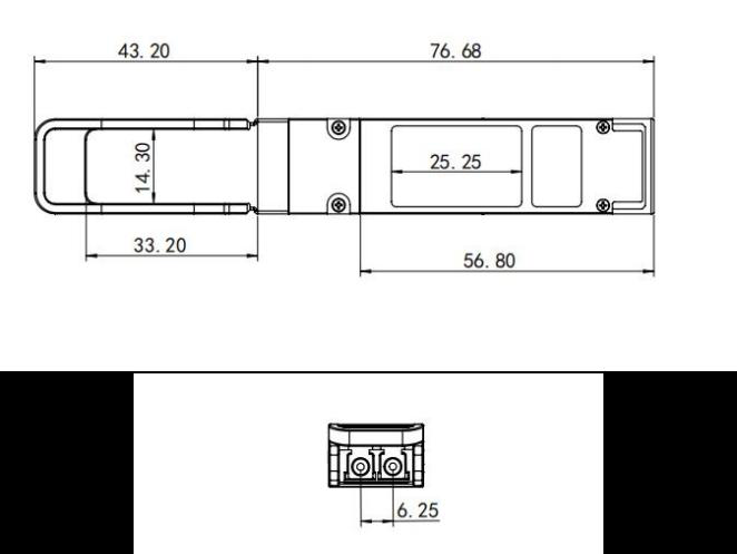
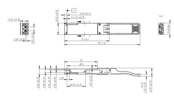
FTQ2-HG-ZRx QSFP28 机械规格符合相关标准要求。拉环颜色为白色(White)。
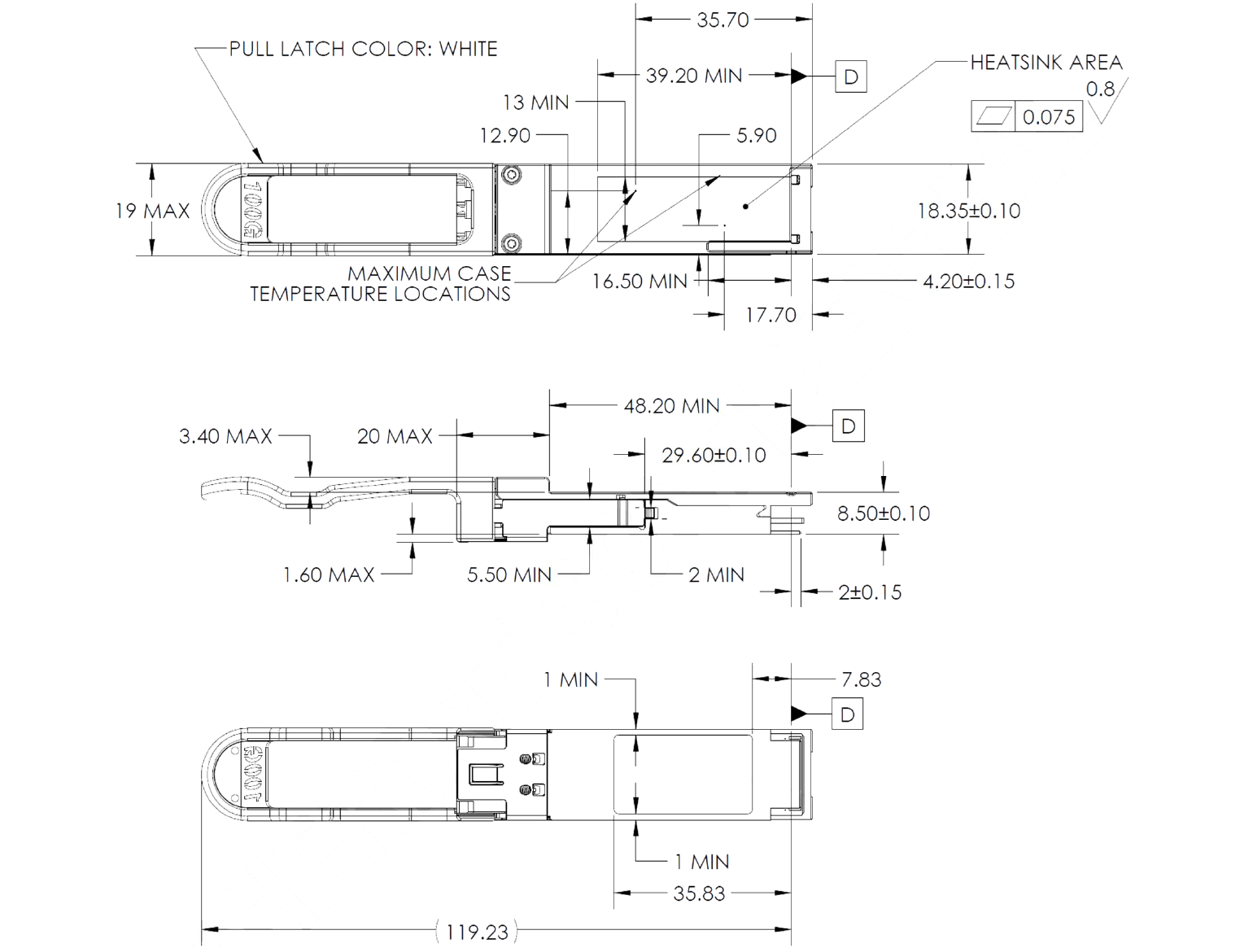
Figure 3 FTQ2-HG-ZRx(x = R/S,t = 1/4)机械外形图
订购信息 / Product Selection
| 产品型号 | 描述 |
|---|---|
| FTQ2-HG-ZR | QSFP28 光模块,100G,ZR,0℃ ~ 70℃ |
| FTQ2-HG-ZRI | QSFP28 光模块,100G,ZR,-40℃ ~ 85℃ |
地区:中国四川天府新区
服务区域:全球
联系方式:
企业电话:028-85255257 | 企业传真:028-85977702 | 企业手机:19081343401
Site:https://www.f-tone.com
人事部:hr@f-tone.com | 市场部:sales@f-tone.com | 技术支持:support@f-tone.com
本产品为100G QSFP28 相干光模块产品线,详细信息,请联系我们的销售人员,谢谢!
Important Notice
Performance figures, data and any illustrative material provided in this data sheet are typical and must be specifically confirmed in writing by F-tone Networks before they become applicable to any particular order or contract. In accordance with the F-tone Networks policy of continuous improvement specifications may change without notice. The publication of information in this data sheet does not imply freedom from patent or other protective rights of F-tone Networks or others. Further details are available from any F-tone Networks sales representative.