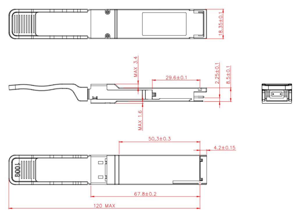
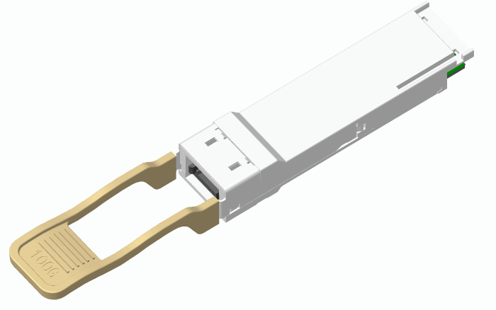
100G QSFP28 SR4 Optical Transceiver
FTQ2-HG-SR4xx
Features
- 4 independent full-duplex channels
- Up to 25.78Gbps data rate per channel
- MPO12 optical connector
- QSFP28 MSA compliant
- Digital diagnostic capabilities
- Up to 100m transmission on OM4 multi-mode ribbon fiber
- Single3.3V power supply
- CML compatible electrical I/O
- International Class1 laser safety certified
- Operating temperature range:
Commercial: 0°C~70°C
Industrial: -40°C~85°C
- RoHS Compliant
Application
- Data center
- 100GBASE-SR4Ethernet
- eCPRI&CPRI
- Other high speed data connections
Standard
- Compliant withSFF-8436
- Compliant withIEEE802.3bm
General Description
The product is designed with form factor, optical/electrical connection and digital diagnostic interface according to the QSFP28 Multi-Source Agreement (MSA). It has been designed to meet the harshest external operating conditions including temperature, humidity and EMI interference. The module offers very high functionality and feature integration, accessible via a two-wire serial interface.
Specification
|
Absolute Maximum Ratings |
||||
|
Parameter |
Symbol |
Min |
Max |
Unit |
|
Storage temperature |
TS |
-40 |
85 |
°C |
|
Power Supply Voltage |
VCC |
-0.5 |
4.0 |
V |
|
Relative Humidity |
RH |
15 |
85 |
% |
|
Receiver Damage Threshold Per Lane |
+3.4 |
dBm |
||
|
Recommended Operating Conditions |
||||||
|
Parameter |
Symbol |
Min |
Typical |
Max |
Unit |
Notes |
|
Operating Case Temperature |
TC |
0 |
70 |
°C |
FTQ2-HG-SR4 |
|
|
-40 |
85 |
FTQ2-HG-SR4I |
||||
|
Power Supply Voltage |
VCC |
3.13 |
3.3 |
3.47 |
V |
|
|
Data Rate(Per channel) |
25.78125 |
Gbps |
||||
|
Control Input Voltage High |
2 |
Vcc |
V |
|||
|
Control Input Voltage Low |
0 |
0.8 |
V |
|||
|
Fiber Length over OM4MMF |
100 |
m |
||||
|
Fiber Length over OM3 MMF |
70 |
m |
||||
|
Power Consumption |
PC |
2.5 |
W |
|||
|
Electrical Characteristics |
||||||
|---|---|---|---|---|---|---|
|
Parameter |
Symbol |
Min |
Typical |
Max |
Unit |
Notes |
|
Total Supply Current |
ICC |
1060 |
mA |
|||
|
Transmitter (each Lane) |
||||||
|
Signaling Speed per Lane |
25.78125 ± 100ppm |
Gbps |
||||
|
Differential Input Voltage tolerance |
900 |
mVpp |
||||
|
Single-ended Input Voltage Tolerance |
-0.35 |
3.3 |
V |
|||
|
Module stress input test |
Per Section 83E.3.4.1, IEEE-802.3bm |
|||||
|
Receiver (each Lane) |
||||||
|
Signaling Speed per Lane |
25.78125 ± 100ppm |
Gbps |
||||
|
Receiver Differential Output Swing |
400 |
800 |
mVpp |
|||
|
Eye Width |
0.57 |
UI |
||||
|
Eye height, differential |
228 |
mV |
||||
|
Vertical eye closure |
VEC |
5.5 |
dB |
|||
|
Transmission time (20% to 80%) |
Tr, Tf |
12 |
ps |
|||
|
Optical Transmitter Characteristics |
|||||||
|
Parameter |
Symbol |
Min |
Typical |
Max |
Unit |
Notes |
|
|
Signaling Speed per Lane |
25.78125 |
Gbps |
|||||
|
Center Wavelength |
λc |
840 |
850 |
860 |
nm |
||
|
RMS Spectral Width |
∆λ |
0.6 |
nm |
||||
|
Average Launch Power per Lane |
PAVG |
-8.4 |
2.4 |
dBm |
|||
|
Transmit OMA per Lane |
POMA |
-6.4 |
3 |
dBm |
|||
|
Average Launch Power of OFF Transmitter per Lane |
-30 |
dBm |
|||||
|
Extinction Ratio |
ER |
2 |
dB |
||||
|
Optical Return Loss Tolerance |
12 |
dB |
|||||
|
Average launch power of OFF Transmitter, each lane |
POFF |
-30 |
dBm |
||||
|
Optical Receiver Characteristics |
|||||||
|
Parameter |
Symbol |
Min |
Typical |
Max |
Unit |
Notes |
|
|
Center Wavelength |
λc |
840 |
850 |
860 |
nm |
||
|
Damage Threshold per Lane |
THD |
3.4 |
dBm |
||||
|
Average receive Power per Lane |
-10.0 |
2.4 |
dBm |
||||
|
Receive Power (OMA) per Lane |
ROMA |
3.0 |
dBm |
||||
|
Stressed Sensitivity (OMA) per Lane |
-5.2 |
dBm |
BER@5e-5 |
||||
|
Receiver Reflectance |
-12 |
dB |
|||||
|
LOS De-assert Level |
LOSD |
-10.5 |
dBm |
||||
|
LOS Assert Level |
LOSA |
-30 |
dBm |
||||
|
LOS hysteresis |
HYS |
0.5 |
dB |
||||
Pin Definition
|
Pin No |
Symbol |
Name/Description |
Notes |
|---|---|---|---|
|
1 |
GND |
Transmitter Ground(Common with Receiver Ground) |
1 |
|
2 |
Tx2n |
Transmitter Inverted Data Input, CML |
|
|
3 |
Tx2p |
Transmitter Non-Inverted Data Input, CML |
|
|
4 |
GND |
Transmitter Ground(Common with Receiver Ground) |
1 |
|
5 |
Tx4n |
Transmitter Inverted Data Input, CML |
|
|
6 |
Tx4p |
Transmitter Non-Inverted Data Input, CML |
|
|
7 |
GND |
Transmitter Ground(Common with Receiver Ground) |
1 |
|
8 |
ModSelL |
Module Select, LVTTL |
|
|
9 |
ResetL |
Module Reset, LVTTL |
|
|
10 |
VccRx |
3.3V Power Supply Receiver |
2 |
|
11 |
SCL |
2-Wire serial Interface Clock |
|
|
12 |
SDA |
2-Wire serial Interface Data |
|
|
13 |
GND |
Transmitter Ground(Common with Receiver Ground) |
|
|
14 |
Rx3p |
Receiver Non-Inverted Data Output, CML |
|
|
15 |
Rx3n |
Receiver Inverted Data Output, CML |
|
|
16 |
GND |
Transmitter Ground(Common with Receiver Ground) |
1 |
|
17 |
Rx1p |
Receiver Non-Inverted Data Output, CML |
|
|
18 |
Rx1n |
Receiver Inverted Data Output, CML |
|
|
19 |
GND |
Transmitter Ground(Common with Receiver Ground) |
1 |
|
20 |
GND |
Transmitter Ground(Common with Receiver Ground) |
1 |
|
21 |
Rx2n |
Receiver Inverted Data Output, CML |
|
|
22 |
Rx2p |
Receiver Non-Inverted Data Output, CML |
|
|
23 |
GND |
Transmitter Ground(Common with Receiver Ground) |
1 |
|
24 |
Rx4n |
Receiver Inverted Data Output, CML |
1 |
|
25 |
Rx4p |
Receiver Non-Inverted Data Output, CML |
|
|
26 |
GND |
Transmitter Ground(Common with Receiver Ground) |
1 |
|
27 |
ModPrsl |
Module Present, LVTTL |
|
|
28 |
IntL |
Interrupt, LVTTL |
|
|
29 |
VccTx |
3.3V power supply transmitter |
2 |
|
30 |
Vcc1 |
3.3V power supply |
2 |
|
31 |
LPMode |
Low Power Mode, LVTTL |
|
|
32 |
GND |
Transmitter Ground(Common with Receiver Ground) |
1 |
|
33 |
Tx3p |
Transmitter Non-Inverted Data Input, CML |
|
|
34 |
Tx3n |
Transmitter Inverted Data Input, CML |
|
|
35 |
GND |
Transmitter Ground(Common with Receiver Ground) |
1 |
|
36 |
Tx1p |
Transmitter Non-Inverted Data Input, CML |
|
|
37 |
Tx1n |
Transmitter Inverted Data Input, CML |
|
|
38 |
GND |
Transmitter Ground(Common with Receiver Ground) |
1 |