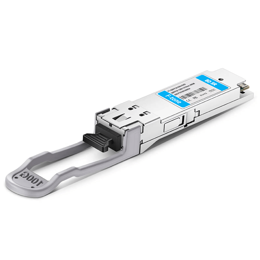
F-tone Networks100G/200G CFP2 DCO Optical Transceiver
FTC2-2H-DCO
Features
- Maximum operating rate of 211.45Gbps
- Modulation format PM-QPSK (100G), PM-16QAM (200G)
- 100GE, OTU4 / OTUCn service access
- Hot-swappable CFP2 package
- Electrical interface supports OTL4.4, FOIC1.4, CAUI-4, and OTLC2.8
- Support the protocol CFP2 MSA Hardware Specification 1.0
- Support the protocol CFP MSA Management Interface Specification 2.2
- Optional proximal distal data loop back
- Support for OTN framer and Ethernet MAC / PCS
- Supports LLDP packet listening
- Maximum power consumption of 24W
- Tunable DWDM C-band, 50GHz ITU grid
- Built-in DSP and FEC (Forward Error Correction)
- Real-time digital diagnostic monitoring
- Single +3.3V power supply
- Compliant with RoHS
- Class 1 laser safety compliant
- EMC compliant
- Case operating temperature:
Commercial: 0 ~ +70℃
Applications
- 100GbE IEEE 802.3bj;
- ITU-T G.709/Y.1331 for Optical transport network
- Switch to switch interface or Switch to router interface
- Access, Metro, Long-haul Ethernet DWDM Networks
- Data Center Interconnect (DCI)
- Carrier Transport Network
- Point-to-point coherent transmission
Description
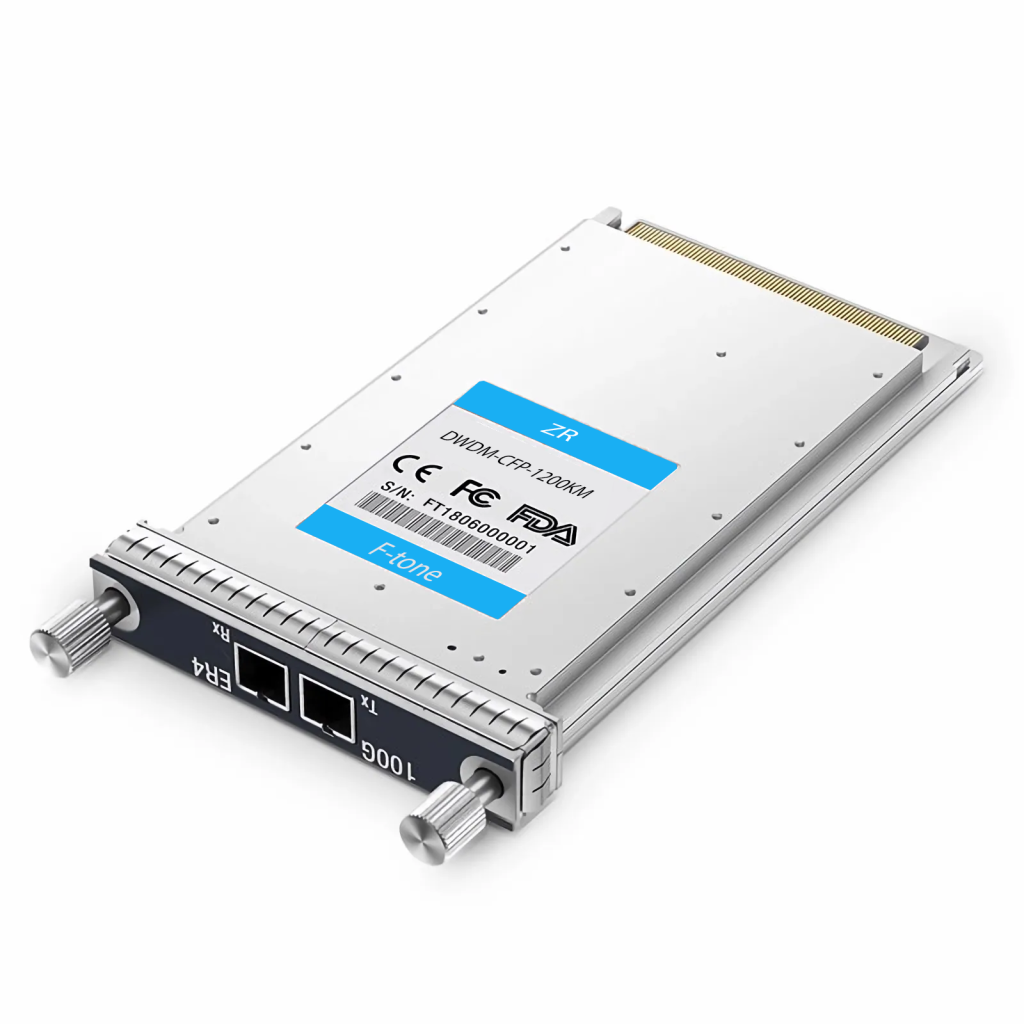
The F-tone Networks 100G/200G CFP2-DCO optical module, using a 104pin CFP2-MSA connector, serves as an electrical interface to the system board. The physical diagram of the module is shown in Figure :
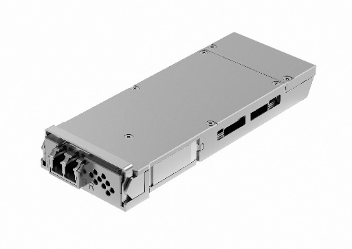
module physical diagram
The module is mainly divided into three main functions: DSP, optical device and control unit. All the control interface pins are implemented by the internal control unit, which can also be used for the terminal modulator control, software management, and alarm performance reporting.
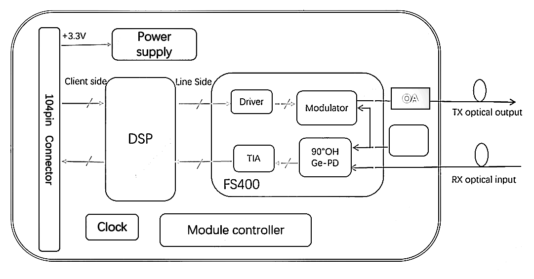
ITLA
Figure Functional block diagram of the CFP 2-DCO optical module performance index
1.1 Optical port characteristics-100G
Table 1 Description of the 100G optical port performance indicators
|
parameter |
Performance value |
|
Optical interface type |
PM-QPSK |
|
Number of wavelength channels |
96 Wave |
|
wavelength interval |
50GHz |
|
wavelength frequency range |
191.3~196.05THz |
|
wavelength stability |
±1.5GHz |
|
Output optical power default value |
0dBm |
|
Output power is a configurable power with a maximum value |
+5dBm |
|
The output power can be configured with a minimum value |
-10dBm |
|
Output power configuration accuracy |
+/-1.5dB |
|
Output Optical power during wavelength regulation |
<-35dBm |
|
CD tolerance |
±40,000ps/nm |
|
Maximum average DGD tolerance |
50ps |
|
Input the optical power range |
0~-18dBm |
|
OSNR tolerances (BOL) |
11.5dB (received Optical power-8~ -10dBm) |
|
power dissipation |
Typ:22W;Max:24W |
1.2 Optical port characteristics-200G
Table 2 Description of 200G optical port performance indicators
|
parameter |
Performance value |
|
Optical interface type |
PM-16QAM PS |
|
Number of wavelength channels |
96 Wave |
|
wavelength interval |
50GHz |
|
wavelength frequency range |
191.3~196.05THz |
|
wavelength stability |
±1.5GHz |
|
Output optical power default value |
0dBm |
|
Output power is a configurable power with a maximum value |
+5dBm |
|
The output power can be configured with a minimum value |
-10dBm |
|
Output power configuration accuracy |
+/-1.5dBm |
|
Output Optical power during wavelength regulation |
<-35dBm |
|
CD tolerance |
±40,000ps/nm |
|
Maximum average DGD tolerance |
22ps |
|
Input the optical power range |
0~-18dBm |
|
OSNR tolerances (BOL) |
17.5dB (received Optical power-8~ -10dBm) |
|
power dissipation |
Typ:22W;Max:24W |
The CFP2 optical module is powered by a separate 3.3V power supply coming from the motherboard. The internal device power supply of the optical module is converted from 3.3V power supply. The 3.3V power supply requirements are shown in Table 3. All the voltages are tested at the connector interface.
Table 2 Power supply characteristics of CFP2 optical module
|
parameter |
Signal name |
least value |
representative value |
crest value |
unit |
remarks |
|
The 3.3V DC power supply voltage is provided |
VCC |
3.2 |
3.3 |
3.4 |
V |
|
|
The 3.3V DC power supply current |
ICC |
8.7 |
A |
Remarks 1 & 2 |
||
|
power supply noise |
Vrip |
2 |
%p-p |
DC – 1MHz |
||
|
3 |
1 – 10MHz |
|||||
|
Power power consumption |
Pw_class 4 |
26 |
29 |
W |
400G pattern |
|
|
working temperature |
T |
0 |
70 |
°C |
Note: The maximum minimum parameter value describes the full temperature range of the module life. Typical parameter values describe the operating temperature of 25°C, normal power supply, and life start indicators.
Note 1: The maximum current value of each pipe pin shall not exceed 1.3A.
Note 2: The maximum value of the Icc is for the design reference, and the normal operating current cannot exceed the Pw_normal / Vcc.
2.2 High-speed electrical interface index
The CFP2 optical module can support a variety of electrical interfaces, as shown in Table 4
Table 4. CFP2 optical module
|
Client Type |
Interface Type |
Electrical Standards |
|
100GE |
CAUI-4 |
IEEE 802.3bm CAUI-4 Chip-to-Module |
|
100GE |
100GAUI-2 |
IEEE 802.3bm GAUI-8 Chip-to-Module |
|
OTU4 |
OTL4.4 |
OIF CEI-28G VSR |
|
OTUC1/OTUC2 |
FOIC1.4(FlexO-SR) |
OIF CEI-28G VSR |
2.2.1. Reference Clock (REFCLK)
The CFP2 optical module does not require the motherboard to provide a reference clock REFCLK of 1 / 16.
2.2.2 Terminal Monitoring Clock (TXMCLK)
The CFP2 optical module hair terminal can selectively provide a monitoring clock TXMCLK, mainly for monitoring the hair terminal Optical signal as a reference. The clock can be used to trigger a high-speed sampling oscilloscope.
Table 5 The Terminal Monitoring Clock (TXMCLK) Characteristics
|
parameter |
Signal name |
least value |
representative value |
crest value |
unit |
remarks |
|
impedance |
Zd |
80 |
100 |
120 |
Ω |
|
|
The terminal monitoring clock frequency TXMCLK |
1/48 |
Hz |
The frequency is 1 / 48 of the symbol rate of the terminal Optical signal |
|||
|
TXMCLK differential voltage |
VDIFFTX |
500 |
1000 |
mV |
Differential peak peak voltage |
2.3.Function description of control pin (non-MDIO port)
2.3.1.1 Non-enable pin (TX_DIS)
Terminal non-enabling pin TX_DIS is an input pin from the motherboard that works in a logical high-level state. When TX_DIS is a logical high level, the output Optical signal inside the optical module is turned off. When TX_DIS is a logic low level, the output Optical signal inside the Optical module is turned on. The timing of the TX_DIS is shown in Figure 7. On time t_on and off time t_off value are shown in Figure 3.
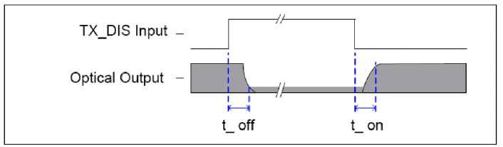
FIG. 3 Time diagram of transmission terminal nonenable signal TX_DIS
2.3.2 Module Low-power pin (MOD_LOPWR)
The optical module low-power pin (MOD_LOPWR) is an input pin from the mainboard that works in a logical high-level state. When the MOD_LOPWR is at a high level, the optical module is in a low-power mode and remains in this mode. When MOD_LOPWR is pulled down, the internal optical module is internally initialized into high power mode or normal operation mode. In the low-power mode, the optical module communicates through the MDIO management interface, and the maximum power consumption of the module does not exceed 2W. The MOD_LOPWR pin timing diagram is shown in Figure 8, with the t_MOD_LOPWR_on and _ t_ MOD_LOPWR_off values shown.
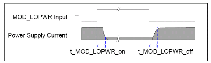
Figure 4 MOD_LOPWR timing diagram of module low power mode
2.3.3 Module reset pin (MOD_RSTn)
The optical module reset pin MOD_RSTn is an input pin from the motherboard and works in a logic-low-level state. When the MOD_RSTn is pulled to low levels, the optical module is reset. When the MOD_RSTn is a high level, the optical module exits the reset mode and starts the module overpower initialization process.
2.4 Function description of alarm pin (non-MDIO port)
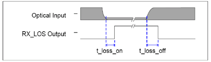
2.4.1 Lost receiver signal alarm pin (RX_LOS)
The receiver signal loss alarm pin RX_LOS is an output output pin connected to the main board and operates in a logical high-level state. When RX_LOS is a logical high level, it indicates that the optical module receives the optical power that is too low. The timing of the RX_LOS pins is shown in Figure