SFP+ LR Transceiver
10.3Gbps 10KM
FTCS-131X-10D
Features
• 10Gb/s serial optical interface compliant to 802.3ae
10GBASE-LR
• Electrical interface compliant to SFF-8431 specifications for enhanced 8.5 and 10 Gigabit
small form factor pluggable module “SFP+”
• 1310nm DFB transmitter, PIN photo-detector
Applications
• High-speed storage area networks
• Computer cluster cross-connect
• Custom high-speed data pipes
• 2-wire interface for management specifications compliant with SFF 8472 digital diagnostic
monitoring interface for optical transceivers
• Operating case temperature:
0 to 70 °C or-40 to 85 °C
• ll-metal housing for superior EMI performance
• Low power consumption
• Advanced firmware allow customer system encryption information to be stored in transceiver
• Cost effective SFP+ solution, enables higher
• port densities and greater bandwidth
• RoHS compliant
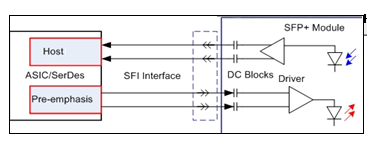
Figure1: Application in System
1. GENERAL DESCRIPTION
This 1310 nm DFB 10Gigabit SFP+ transceiver is designed to transmit and receive optical data over single
mode optical fiber for link length 10km.
The SFP+ LR module electrical interface is compliant to SFI electrical specifications. The transmitter input and
receiver output impedance is 100 Ohms differential. Data lines are internally AC coupled. The module provides
differential termination and reduce differential to common mode conversion for quality signal termination and low
EMI. SFI typically operates over 200 mm of improved FR4 material or up to about 150mmof standard FR4 with one
connector.
The transmitter converts 10Gbit/s serial CML electrical data into serial optical data compliant with the
10GBASE-LR standard. An open collector compatible Transmit Disable (Tx_Dis) is provided. A logic “1,” or
no connection on this pin will disable the laser from transmitting. A logic “0” on this pin provides normal
operation. The transmitter has an internal automatic power control loop (APC) to ensure constant optical
power output across supply voltage and temperature variations. An open collector compatible Transmit Fault
(TFault) is provided. TX_Fault is a module output contact that when high, indicates that the module transmitter
has detected a fault condition related to laser operation or safety. The TX_Fault output contact is an open
drain/collector and shall be pulled up to the Vcc_Host in the host with a resistor in the range 4.7-10 kΩ.
TX_Disable is a module input contact. When TX_Disable is asserted high or left open, the SFP+ module
transmitter output shall be turned off. This contact shall be pulled up to VccT with a 4.7 kΩ to 10 kΩ resistor
The receiver converts 10Gbit/s serial optical data into serial PECL/CML electrical data. An open collector
compatible Loss of Signal is provided. Rx_LOS when high indicates an optical signal level below that specified
in the relevant standard. The Rx_LOS contact is an open drain/collector output and shall be pulled up to
Vcc_Host in the host with a resistor in the range 4.7-10 kΩ, or with an active termination. Power supply
filtering is recommended for both the transmitter and receiver. The Rx_LOS signal is intended as a
preliminary indication to the system in which the SFP+ is installed that the received signal strength is below the
specified range. Such an indication typically points to non-installed cables, broken cables, or a disabled, failing
o r a powered off transmitter at the far end of the cable.
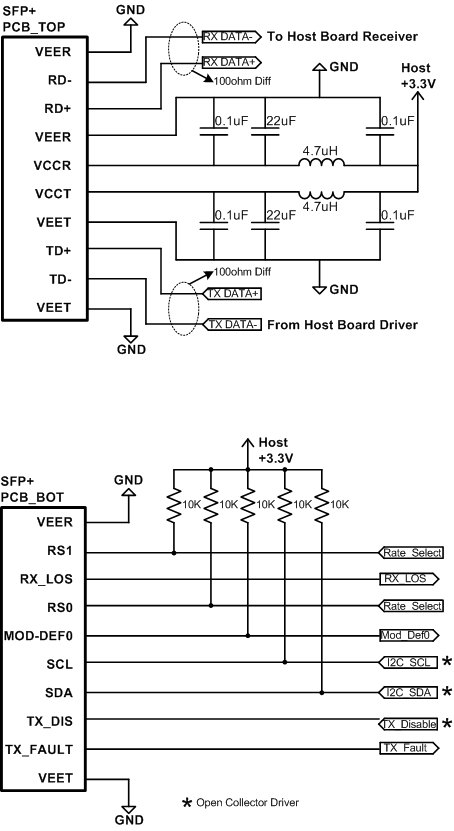
2. PROPOSED APPLICATION SCHEMATICS
3. PIN DEFINITION
The SFP+ modules are hot-pluggable. Hot pluggable refers to plugging in or unplugging a module while the
host board is powered. The SFP+ host connector is a 0.8 mm pitch 20 position right angle improved connector
specified by SFF-8083, or stacked connector with equivalent with equivalent electrical performance. Host
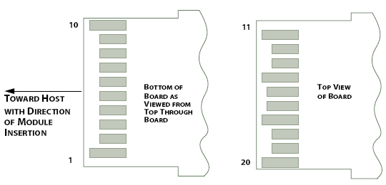
PCB contact assignment is shown in Figure 2 and contact definitions are given in Table 2. SFP+ module
contacts mates with the host in the order of ground, power, followed by signal as illustrated by Figure 3 and the
contact sequence order listed in Table 2.
Figure 2: Module Interface to Host
Figure 3: Module Contact Assignment
PIN Logic Symbol Name / Description Note
1 VeeT Module Transmitter Ground 1
2 LVTTL-O TX_Fault Module Transmitter Fault
Transmitter Disable; Turns off transmitter laser
3 LVTTL-I TX_Dis output
4 LVTTL-I/O SDA 2-Wire Serial Interface Data Line 2
5 LVTTL-I SCL 2-Wire Serial Interface Clock 2
6 MOD_DEF0 Module Definition, Grounded in the module
7 LVTTL-I RS0 Receiver Rate Select
8 LVTTL-O RX_LOS Receiver Loss of Signal Indication Active LOW
9 LVTTL-I RS1 Transmitter Rate Select (not used)
10 VeeR Module Receiver Ground 1
11 VeeR Module Receiver Ground 1
12 CML-O RD- Receiver Inverted Data Output
13 CML-O RD+ Receiver Data Output (not used)
14 VeeR Module Receiver Ground 1
15 VccR Module Receiver 3.3 V Supply
16 VccT Module Receiver 3.3 V Supply
17 VeeT Module Transmitter Ground 1
18 C ML-I TD+ Transmitter Non-Inverted Data Input
19 C ML-I TD- Transmitter Inverted Data Input
20 VeeT Module Transmitter Ground 1
Table 2: SFP+ Module PIN Definition
Note:
1. Module ground pins GND are isolated from the module case.
2. Shall be pulled up with 4.7K-10Kohms to a voltage between 3.15V and 3.45V on the host board.
4. TRANSCEIVER BLOCK DIAGRAM
5. ABSOLUTE MAXIMUM RATING
These values represent the damage threshold of the module. Stress in excess of any of the individual
Absolute Maximum Ratings can cause immediate catastrophic damage to the module even if all other
parameters are within Recommended Operating Conditions.
Parameters Symbol Min. Max. Unit
PowerSupplyVoltage V 0 3.6 V
CC
StorageTemperature Tc -40 85 C
Tc 0 70
Operating Case Temperature C
TI -40 85
RelativeHumidity RH 5 95 %
R XInputAveragePower Pmax – 0 dBm
Table 3: Absolute Maximum Rating
6. RECOMMENDED OPERATING ENVIRONMENT
Recommended Operating Environment specifies parameters for which the electrical and optical characteristics
hold unless otherwise noted.
Parameters Symbol Min. Typical Max Unit
PowerSupplyVoltage V 3.135 3.3 3.465 V
CC
PowerSupplyCurrent Icc 300 mA
T 0 25 70
Operating Case C
C
Temperature
TI -40 25 85
Table 4: Recommended Operating Environment
7. OPTICAL CHARACTERISTICS
The follo wing optical characteristics are defined over the Recommended Operating Environment unless
otherwise specified.
Parameters Unit Values
Operating Reach m 2 – 10K
Transmitter
Center wavelength (range) nm 1260 -1355
Side Mode Suppression Ratio (min) dB 30
Launched power
– maximum (Average) dBm 0.5
– minimum (Average) dBm -8.2
OMA(min) dBm -5.2
OMA-TDP (min) dBm -6.2
Transmitter and dispersion penalty (max) dB 3.2
Average launch power of OFF transmitter (max) dBm -30
Extinction ratio (min) dB 3.5
RIN12 OMA (max) dB/Hz -128
Optical Return Loss Tolerance (min) dB 12
Receiver
Center wavelength (range) nm 1260-1355
Receive overload (max) in average power(note 1) dBm 0.5
Receive sensitivity (min) in average power(note 1 ) dBm -14.4
Receiver sensitivity (max) in OMA (note 2) dBm -12.6
Receiver Reflectance (max) dB -12
Stressed receiver sensitivity (max) in OMA(note 2) dBm -10.3
Vertical eye closure penalty (min)(note 3) dB 2.2
Los Assert(min) dBm -30
Los Dessert(max) dBm -12
Los Hysteresis(min) dB 0.5
Stressed eye jitter (min)(note 2) UIp-p 0.3
Receive electrical 3dB upper cutoff frequency (max) GHz 12.3
Receiver power (damage, Max) dBm 1.5
Notes:
1. Average optical power shall be measured using the methods specified in TIA/EIA-455-95.
2. Receiver sensitivity is informative. Stressed receiver sensitivity shall be measured with conformance test signal for BER =1x
10-12 .
3. Vertical eye closure penalty and stressed eye jitter are the test conditions for measuring stressed receiver sensitivity. They are
not the required characteristic of the receiver.
4. Power budget is defined as the different between the Rx sensitivity and the Tx output power of the interface.
5. Path penalty is intended as the power penalty of the interface between back-to-back and the maximum applied dispersion.
Table 5: Optical Characteristics
8. DITITAL DIAGNOSTIC FUNCTIONS
The following digital diagnostic characteristics are defined over the Recommended Operating Environment
unless otherwise specified. It is compliant to SFF8472 Rev10.2 with internal calibration mode. For external
calibration mode please contact our sales stuff.
Parameter Symbol Min. Max Unit Notes
Over
Temperature monitor
DMI_Temp -3 3 degC operating
absolute error
temp
Laser power monitor
DMI_TX -3 3 dB
absolute error
• 1dBm to
RX power monitor
DMI_RX -3 3 dB -15dBm
absolute error
range
Full
Supply voltage monitor
DMI_VCC -0.08 0.08 V operating
absolute error
range
Biascurrentmonitor DMI_Ibias -10% 10% mA
Table 7: Digital diagnostic specification table
9. ELECTRICAL CHARACTERISTICS
The following electrical characteristics are defined over the Recommended Operating Environment unless
otherwise specified.
Parameter Symbol Min. Typical Max Unit Notes
DataRate – 10.3125 – Gbps
PowerConsumption – 800 1000 mW
Transmitter
Single Ended Output
• 0.3 4 V
Voltage Tolerance –
C common mode
15 mV
voltage tolerance – –
TxInputDiffVoltage VI 180 800 mV
TxFault VoL -0.3 0.4 V At0.7mA
Data Dependent Input
DDJ 0.1 UI
Jitter
DataInputTotalJitter TJ 0.28 UI
Receiver
Single Ended Output
• 0.3 4 V
Voltage Tolerance –
RxOutputDiffVoltage Vo 300 850 mV
Rx Output Rise and Fall 20% to
Tr/Tf 30 ps
Time 80%
TotalJitter TJ 0.7 UI
Deterministic Jitter DJ 0.42 UI
Table 8: Electrical Characteristics
10. CONTROL AND STATUS I/O TIMING CHARACTERISTICS
Timing characteristics of control and status I/O are included in Table 8, which is also defined in SFF-8431.
Table 9: Timing Characteristics
11. MECHANICAL
Table 10: Key Mechanical Dimensions
12. ESD
This transceiver is specified as ESD threshold 2kV for all electrical input pins, tested per MIL-STD-883, Method
3015.4 /JESD22-A114-A (HBM). However, normal ESD precautions are still required during the handling of
this module. This transceiver is shipped in ESD protective packaging. It should be removed from the packaging
and handled only in an ESD protected environment.
13. LASE R SAFTY
This is a Class 1 Laser Product according to IEC 60825-1:1993:+A1:1997+A2:2001. This product complies
with 21 CFR 1040.10 and 1040.11 except for deviations pursuant to Laser Notice No. 50, dated (July 26, 2001)
14. Order Information
Part Number Product Description
FTCS-131X-10D SFP+ Transceiver, 1310nm, 10Gbps, 10km, with DDM, 0°C~+70°C
Important Notice
Performance figures, data and any illustrative material provided in this data sheet are
typical and must be specifically confirmed in writing by F-tone Networks before they
become applicable to any particular order or contract. In accordance with the F-tone
Networks policy of continuous improvement specifications may change without notice.
The publication of information in this data sheet does not imply freedom from patent or
other protective rights of F-tone Networks or others. Further details are available from any
F-tone Networks sales representative.
Detailed Specifications
Product Images
Important Notice
The information contained in this document is the property of Beijing E-Font Communication Technology Co., Ltd. and is provided for technical reference only. Performance parameters are subject to actual test results. For any questions, please contact our technical support.