CFP2 DWDM 100G & CFP2 DWDM 200G Coherent Optical Module
200G 1300km / 100G 3000km CFP2 Coherent Transceiver
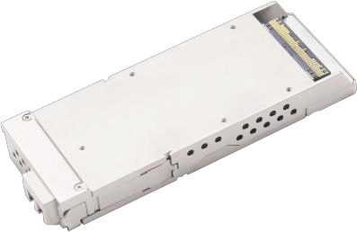
200G1300km/ 100G3000kmCFP2 Coherent
CFP2 DWDM 100G / CFP2 DWDM 200G
Product Features
● Transmissionreachbeyond1300km/3000
km over SMF for 200G/100G
● Hot-pluggable
● Support PM-16QAM(2 00G)a ndPM-
DQPSK/PM-QPSK (100G) modulation
● Supports SD-FEC
● Supports 100G/200 G Flex-rate
● Supports OTU4/OTUC2/2 x 100GE/ 100GE
signaling
● Complian t with CE I-28G-MR sp ecifica tion s
● Complian t with OTL4.4/OTLC2/CAUI-4
signaling
● Complian t with CFP2 MSA Hardware
Specification Rev. 1.0
● Compliant with OI F-CFP2-DCO-01.0
● Complia nt with CFP MSA Management
Interface SpecificationVersion2 .6(R06a)
● Powerco nsumption: 26W (200G)/21W
(100G)
Application
The module is designed to be used on the host board of system integrators to
support transmission over DWDM links in Metro networks. it comprises high-data
lanes, asingle reference clock from hosts, a single 3.3 V power supply, an MDIO in
terface for module control and status report, and
dedicated alarm and control pins.
V 3.06
1 /20
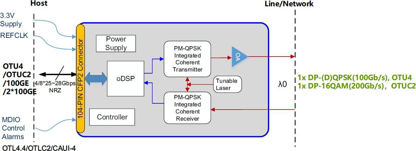
The CFP2 DWDM 100G / CFP2 DWDM 200G module uses a 104-pin CFP2 MSA connector for
all electrical interfaces with the host card, whereas the optical interfaces on the line side
are provided through the optical receptacles on the CFP2. The mod ule can be portioned in
tothree functional parts:Txpath, Rxpath andcontrol&powerblock.
All control interface pins are routed to the MCU and oDSP. The MCU is also used
for fast controls inside the module such as modulator bias adjustment, software
image management, overall control coordination and status reporting.
CFP2 DWDM 100G / CFP2 DWDM 200G block diagram
Host Interface Configuration
The module supports host signal types: OTUC2/OTU4/100GE/2 x 100GE. The host e
lectrical interfaces are compliant with CEI-28G-MR. The host rate is dependent on
the framing type and the supported host rates are shown in the following
table. Clock source is need for synchronization, and module REFCLK input clock =
Host Baud Rate/160.
Host rates
HostFrame Host Data Signaling DataRate REFCLKClock
Rate (Gbps) (Gbps)
200G OTUC2 2 x 112.305 OTLC2NRZ 28.076 175.476 MHz,
±20 ppm
100G OTU4 111.81 OTL4.4NRZ 27.952 174.703 MHz,
±20 ppm
100GE 103.125 CAUI-4 NRZ 25.78125 NA
V 3.06
2 /20
| HostFrame | Host Data Rate (Gbps) |
Signaling | DataRate (Gbps) |
REFCLKClock |
| 200G OTUC2 | 2 x 112.305 | OTLC2NRZ | 28.076 | 175.476 MHz, ±20 ppm |
| 100G OTU4 | 111.81 | OTL4.4NRZ | 27.952 | 174.703 MHz, ±20 ppm |
| 100GE | 103.125 | CAUI-4 NRZ | 25.78125 | NA |
Line Framing Format
The line framing format is F-tone proprietary and it is required that both ends of t
he optical connection use F-tone technologies, in which there is proprietary SD-FE
C in conjunction with 200G PM-16QAM/100G PM-DQPSK/100G PM-QPSK
modulation.
The actual line rate depends on the configured FEC mode and the host data
format.
Line modulation formats
LineData MinGrid BaudRate Modulation FECOH RxOSNR
Rate Spacing (Gbaud) Format (dB) EOL
(GHz) @Pre-FEC
BER
200G 50 39.7 PM-16QAM 25% 17
PM-QPSK
100G 50 33.6 25% 11.5/13
/PM-DQPSK
Configuration Overview
The table below summarizes the possible combinations of host type and line side
(modulation) that can be configured through the MDIO interface. Refer to the CFP
2 DWDM 100G / CFP2 DWDM 200Gsoftware interface specification for register
details needed to configure the CFP2 for the desired application.
Configuration overview table
Host Line Side
HostFormat Signaling Configuration FEC
OTUC2 OTLC2 PM-16QAM SD-FEC
OTU4 OTL4.4 PM-DQPSK SD-FEC
OTU4 OTL4.4 PM-QPSK SD-FEC
2x OTU4 OTL4.4 PM-16QAM SD-FEC
2x 100GE 2 x CAUI-4 PM-16QAM SD-FEC
100GE CAUI-4 PM-QPSK SD-FEC
100GE CAUI-4 PM-DQPSK SD-FEC
V 3.06
3 /20
| LineData Rate |
MinGrid Spacing (GHz) |
BaudRate (Gbaud) |
Modulation Format |
FECOH | RxOSNR (dB) EOL @Pre-FEC BER |
| 200G | 50 | 39.7 | PM-16QAM | 25% | 17 |
| 100G | 50 | 33.6 | PM-QPSK /PM-DQPSK |
25% | 11.5/13 |
| HostFormat | Host Signaling |
Line Side Configuration |
FEC |
| OTUC2 | OTLC2 | PM-16QAM | SD-FEC |
| OTU4 | OTL4.4 | PM-DQPSK | SD-FEC |
| OTU4 | OTL4.4 | PM-QPSK | SD-FEC |
| 2x OTU4 | OTL4.4 | PM-16QAM | SD-FEC |
| 2x 100GE | 2 x CAUI-4 | PM-16QAM | SD-FEC |
| 100GE | CAUI-4 | PM-QPSK | SD-FEC |
| 100GE | CAUI-4 | PM-DQPSK | SD-FEC |
Environmental Specifications
The table below defines the environmental specifications of the CFP2 DWDM 100G/
CFP2 DWDM 200Gmodule.
Environmental Specifications
Parameter Min Max Unit Condition
Environmental –40 85 °C –
storage
Temperature
Environmental – 85 % –
storage(relative)
humidity
Environmental – 85 % –
operating
(relative)
humidity
Operating 0 75 °C This temperature is
temperature monitored through an
internal thermal sensor
(MDIO register B02F). The
temperature reading
represents the module case
temperatureatthespecified
location.
Short term
–
80 ° C T he modu le operates up to a m
operating at high t aximum temperature for
emperature short term (96 hours
continuously, less than 15
days per year). This
te mperature is monitored
through an internal thermal
sensor (MDIO register B02F). Th
e temperature reading
represents the module case
temperature at the specified lo
cation.
V 3.06
4 /20
| Parameter | Min | Max | Unit | Condition |
| Environmental storage Temperature |
–40 | 85 | °C | – |
| Environmental storage(relative) humidity |
– | 85 | % | – |
| Environmental operating (relative) humidity |
– | 85 | % | – |
| Operating temperature |
0 | 75 | °C | This temperature is monitored through an internal thermal sensor (MDIO register B02F). The temperature reading represents the module case temperatureatthespecified location. |
| Short term operating at high t emperature |
– | 80 | ° C | T he modu le operates up to a m aximum temperature for short term (96 hours continuously, less than 15 days per year). This te mperature is monitored through an internal thermal sensor (MDIO register B02F). Th e temperature reading represents the module case temperature at the specified lo cation. |
Absolute Maximum Ratings
Operating or handling the module out of any specified absolute maximum rating
is subject to permanent damage of the module.
Absolutemaximumoperatingconditions
Parameter Min Max Unit Condition
Operatingcase –10 85 °C This temperature is
temperature monitored through an
internal thermal sensor
(MDIO register). The
temperature reading
represents the module case
temperatureatthespecified
locat ion.
Power supply –0.3 3.7 V –
Rx input power – 14 dBm Same modulation format;
same wavelength as Rx local
oscillator;continuousorpeak
power
Electrical Characteristics
A single +3.3 V power supply shall be provided by the host card through the 104-
pin connector and internal DC/DC power converters are used to regulate the
power for different components inside the module. The +3.3 V power supply
provided by the host shall adhere to the CFP2 MSA Hardware Specification
.Theelectric algro undis isolate dfromthe m odule chass is ground.
The power supply requiremen ts are specified in below. Those powe r classes fo
r which the maximum current per pin exceeds 1125 mA will require
agreement from the electrica l connector supplier.
V 3.06
5 /20
| Parameter | Min | Max | Unit | Condition |
| Operatingcase temperature |
–10 | 85 | °C | This temperature is monitored through an internal thermal sensor (MDIO register). The temperature reading represents the module case temperatureatthespecified locat ion. |
| Power supply | –0.3 | 3.7 | V | – |
| Rx input power | – | 14 | dBm | Same modulation format; same wavelength as Rx local oscillator;continuousorpeak power |
Electricalpowerspecifications
Parameter Symbol Min Typ Max Unit Note
3.3 V DC supply P3V3 3.2 3.3 3.4 V Measured at
voltage the
electrical
connector
3.3 V DC supply P3V3_Icc – – 9 A The
current maximum
current/pin
shall not
exceed
1.125 A
Powersupply P3V3_noise – – 2 %p-p DC-500
noise MHz
Powersupply P3V3_rippl e – – 1 %p-p DC-20MHz
ripple
lnrush current P3V3_Iir – – 500 mA/ –
μs
Turn-offcurrent P3V3_Ito –500 – – mA/ –
μs
Pwlp 2 W
Power – – Lo wpower m
consumption ode
Power Pwc4 26*1,*2 W
– – 200G
consumption
PM-16QAM
21*1,*2 W 100G PM-DQ
– –
PSK/ QPSK
NOTE
*1Powerconsu mptiondependsontheactua lapp lication condition .For200GPM-1 6QAM t
ypicalapplic ation,opticallinksshouldhaveenoughOSNRmarginwithpre-BERbetter th
an1.5e-2andpowerconsumptionislessthan26W(200Gwithframerenabled)/21W (10
0G with frame r enabled).
*2Withframe rdisabled,thepowerconsumptionwillbereducedto25Wfor200Gor20W
for 100G.
The CFP2 DWDM 100G / CFP2 DWDM 200Gmodule supports alarm, control, and
monitoring functions over an MDIO bus. This interface consists of eight pins listed
in the table below.
V 3.06
6 /20
| Parameter | Symbol | Min | Typ | Max | Unit | Note |
| 3.3 V DC supply voltage |
P3V3 | 3.2 | 3.3 | 3.4 | V | Measured at the electrical connector |
| 3.3 V DC supply current |
P3V3_Icc | – | – | 9 | A | The maximum current/pin shall not exceed 1.125 A |
| Powersupply noise |
P3V3_noise | – | – | 2 | %p-p | DC-500 MHz |
| Powersupply ripple |
P3V3_rippl e | – | – | 1 | %p-p | DC-20MHz |
| lnrush current | P3V3_Iir | – | – | 500 | mA/ μs |
– |
| Turn-offcurrent | P3V3_Ito | –500 | – | – | mA/ μs |
– |
| Power consumption |
Pwlp | – | – | 2 | W | Lo wpower m ode |
| Power consumption |
Pwc4 | – | – | 26*1,*2 | W | 200G PM-16QAM |
| – | – | 21*1,*2 | W | 100G PM-DQ PSK/ QPSK |
MDIO pins
Signal I/O Logic Description
MDC I 1.2VLVCMOS Managementdataclock,
max. 4 MHz
MDIO I /O 1.2VLVCMOS Managementdatainput
output, max. 4 Mbps
PRTADR[2:0] I 1.2VLVCMOS Physical port address
GLB_ALRMN O 3.3VLVCMOS Global alarm, active low,
indicating FAWS condition
There are six control pins as listed in the following table to support real-time
control via ha rdwar e pins.
Host-control pins
Signal I/O Logic Description
MOD_RSTN I 3.3VLVCMOS Modulereset,activeL,
internal PD
TX_DIS I 3.3VLVCMOS Transmitterdisable,active
H, internal PU
MOD_LOPWR I 3.3VLVCMOS Modulelowpower,active H,
internal PU
PRG_CNTL[2:1] I 3.3VLVCMOS Programmablecontro l[2:1],
internal PU
The PRG_CNTRL [2:1] signals have MSA defined default meanings that are listed
in the CFP MSA implementation agreement. The lower two bits (hardware
interlock) define the power class of the module and must be kept static during
initialization. When MOD_LOPWR is active, the maximum power consumption is <
2 W and the host can still communicate with the module via the MDIO interface.
The MOD_RSTN signal is run to a reset chip to generate a reset to the internal
MCU and oDSP ASIC (RST_N).There are five alarm pins from the module back to
the host.
V 3.06
7 /20
| Signal | I/O | Logic | Description |
| MDC | I | 1.2VLVCMOS | Managementdataclock, max. 4 MHz |
| MDIO | I /O | 1.2VLVCMOS | Managementdatainput output, max. 4 Mbps |
| PRTADR[2:0] | I | 1.2VLVCMOS | Physical port address |
| GLB_ALRMN | O | 3.3VLVCMOS | Global alarm, active low, indicating FAWS condition |
| Signal | I/O | Logic | Description |
| MOD_RSTN | I | 3.3VLVCMOS | Modulereset,activeL, internal PD |
| TX_DIS | I | 3.3VLVCMOS | Transmitterdisable,active H, internal PU |
| MOD_LOPWR | I | 3.3VLVCMOS | Modulelowpower,active H, internal PU |
| PRG_CNTL[2:1] | I | 3.3VLVCMOS | Programmablecontro l[2:1], internal PU |
Module-hostalarmpins
Signal I/O Logic Descr iption
RX_LOS O 3.3VLVCMOS Receiverlossofsignal,
active H
MOD_ABS O 3.3VLVCMOS Moduleabsent,activeH,
internal PD
PRG_ALRM[2:1] O 3.3VLVCMOS Programmable alarm [2:1]
All signals but MOD_ABS interface to the DSP ASIC. The PRG_ALRM [2:1] signals
have MSA defined default meanings that are listed in the CFP2 implementation
agreement.
The transmitter and receiver comply with the CEI-28G-MR electrical specification.
The data lines are AC-coupled and terminated in the module according to the
following figure fr om the CFP2 MSA. The termination also applies to the reference
clock, TX monitor clock, and RX monitor clock.
Transmitterele ctricaloutputch aracteristics
Parameter Symbol Min Typ Max Unit No tes
Signaling rate per TBaud 25.78 – 28.3 Gbps CEI-28G-MR
lane
Differential TVdiff 800 – 1200 mVpp –
voltagepk-pk
Differential TRD 80 100 120 Ω –
output Impedance
Commonmode noi Vrms / / / mV AC-coupled
se (RMS)
Trise/Tfall – TBD –
Transitiontime ps 20% to 80%
Commonreturn los TSCC22
– – –6 dB < 10 GHz
s
–4 dB 10GHz~Baud
– –
Rate
Totaljitter – – – 0.28 UIpp –
V 3.06
8 /20
| Signal | I/O | Logic | Descr iption |
| RX_LOS | O | 3.3VLVCMOS | Receiverlossofsignal, active H |
| MOD_ABS | O | 3.3VLVCMOS | Moduleabsent,activeH, internal PD |
| PRG_ALRM[2:1] | O | 3.3VLVCMOS | Programmable alarm [2:1] |
| Parameter | Symbol | Min | Typ | Max | Unit | No tes |
| Signaling rate per lane |
TBaud | 25.78 | – | 28.3 | Gbps | CEI-28G-MR |
| Differential voltagepk-pk |
TVdiff | 800 | – | 1200 | mVpp | – |
| Differential output Impedance |
TRD | 80 | 100 | 120 | Ω | – |
| Commonmode noi se (RMS) |
Vrms | / | / | / | mV | AC-coupled |
| Transitiontime | Trise/Tfall | – | TBD | – | ps | 20% to 80% |
| Commonreturn los s |
TSCC22 | – | – | –6 | dB | < 10 GHz |
| – | – | –4 | dB | 10GHz~Baud Rate |
||
| Totaljitter | – | – | – | 0.28 | UIpp | – |
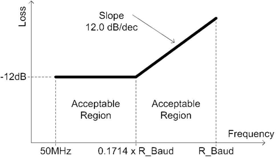
Transmitterdiff return loss mask
Receiverelectricalinputcharacteristics
Parameter Symbol Min Typ Max Unit Notes
Signaling rate per la
ne RBaud 25.78 – 28.3 Gbps CEI-28G-MR
Compliant
Differential with
RVdiff – TBD – mVppd
voltagepk-pk CEI-28G-MR
Commonmode nois
e (RMS) Vrms – TBD – mV AC coupled
– –
Transitiontime Trise/Tfall TBD ps 20% to 80%
Differentialin put im
pedance RRD 80 100 120 Ω –
– – –6 dB < 1 0 GHz
Commonreturn loss RSCC11 10
– – –4 dB
GHz~ Baud Ra
te
Sinusoidaljitter, max
imum R_SJ-max – – 5 UIpp –
Sinusoidaljitter, hig
h frequency R_SJ-hi – – 0.05 UIpp –
Offset of frequency
– – – 20/100 ppm OTN/ETH
V 3.06
9 /20
| Parameter | Symbol | Min | Typ | Max | Unit | Notes |
| Signaling rate per la ne |
RBaud | 25.78 | – | 28.3 | Gbps | CEI-28G-MR |
| Differential voltagepk-pk |
RVdiff | – | TBD | – | mVppd | Compliant with CEI-28G-MR |
| Commonmode nois e (RMS) |
Vrms | – | TBD | – | mV | AC coupled |
| Transitiontime | Trise/Tfall | – | TBD | – | ps | 20% to 80% |
| Differentialin put im pedance |
RRD | 80 | 100 | 120 | Ω | – |
| Commonreturn loss | RSCC11 | – | – | –6 | dB | < 10 GHz |
| – | – | –4 | dB | 10 GHz~ Baud Ra te |
||
| Sinusoidaljitter, max imum |
R_SJ-max | – | – | 5 | UIpp | – |
| Sinusoidaljitter, hig h frequency |
R_SJ-hi | – | – | 0.05 | UIpp | – |
| Offset of frequency | – | – | – | 20/100 | ppm | OTN/ETH |
Receiverdiff return loss mask
Optical Characteristics
All specifications given in this document are End-of-Life numbers and are valid
over the operating temperature. The two tables below contain specifications of the
general transmitter and the general receiver.
Opticaltransmitter specifications
Parameter Min Typ Max Unit Condition
Transmitter ITU-T 50GHzgr
191.3 196.1 THz
frequencyrange – id
Transmitter laser f
–1.5 1.5 GHz
– –
requencystability
Transmitter
–10 – 1 dBm Tunable,
outputpower rang
default0.5 dBm
e
Output power
–0.3 0.3 dB
– –
stability(standard
range)
Output power
–1 1 dB
– –
accuracy and
stability(standard
range)
Transmitterlaser di
10 ms
sable time – – –
Transmitter
60 s
wavelength – – –
switchingtime
Transmitter turn-u
60 120 s
– –
ptimefromcold s
tart
V 3.06
10/20
| Parameter | Min | Typ | Max | Unit | Condition |
| Transmitter frequencyrange |
191.3 | – | 196.1 | THz | ITU-T 50GHzgr id |
| Transmitter laser f requencystability |
–1.5 | – | 1.5 | GHz | – |
| Transmitter outputpower rang e |
–10 | – | 1 | dBm | Tunable, default0.5 dBm |
| Output power stability(standard range) |
–0.3 | – | 0.3 | dB | – |
| Output power accuracy and stability(standard range) |
–1 | – | 1 | dB | – |
| Transmitterlaser di sable time |
– | – | 10 | ms | – |
| Transmitter wavelength switchingtime |
– | – | 60 | s | – |
| Transmitter turn-u ptimefromcold s tart |
– | 60 | 120 | s | – |
Parameter Min Typ Max Unit Condition
TransmitterOSNR 35 – – dB/0.1 nm OSNR at
transmitter
output (in-
band)
Transmitter TBD – – dB/0.1 nm Signal to the
signal-to-max ASE maximumout-
of-band ASE
level
Transmitter 24 – – dB –
opticalreturnloss
Transmitter – – –35 dBm E.g., max.
output power output power
withTXdisabled when
changing laser
frequency.
Transmitter – – 1 dB Power
polarization d eference
dependentpower betweenXand
Y polarization
Opticalreceiverspecification
Parameter Min Typ Max Unit Condition
Receiver 191.3 – 196.1 THz –
frequencyrange
Optimuminput –14 – 0 dBm Signal power
power range oftheselected
channel. The
input power
range gets
optimum
OSNR
performance
Extendedinput –18 – 0 dBm @0.5dBOSNR
power range penalty
OSNRtolerance – 16.2 16.7 dB/0.1 nm 200G
(BOL) PM-16QAM
– 10.6 11 dB/0.1 nm 100GPM-
QPSK
– 12.3 12.8 dB/0.1 nm 100GPM-
DQPSK
V 3.06
11/20
| Parameter | Min | Typ | Max | Unit | Condition |
| TransmitterOSNR | 35 | – | – | dB/0.1 nm | OSNR at transmitter output (in- band) |
| Transmitter signal-to-max ASE |
TBD | – | – | dB/0.1 nm | Signal to the maximumout- of-band ASE level |
| Transmitter opticalreturnloss |
24 | – | – | dB | – |
| Transmitter output power withTXdisabled |
– | – | –35 | dBm | E.g., max. output power when changing laser frequency. |
| Transmitter polarization dependentpower |
– | – | 1 | dB | Power d eference betweenXand Y polarization |
| Parameter | Min | Typ | Max | Unit | Condition |
| Receiver frequencyrange |
191.3 | – | 196.1 | THz | – |
| Optimuminput power range |
–14 | – | 0 | dBm | Signal power oftheselected channel. The input power range gets optimum OSNR performance |
| Extendedinput power range |
–18 | – | 0 | dBm | @0.5dBOSNR penalty |
| OSNRtolerance (BOL) |
– | 16.2 | 16.7 | dB/0.1 nm | 200G PM-16QAM |
| – | 10.6 | 11 | dB/0.1 nm | 100GPM- QPSK |
|
| – | 12.3 | 12.8 | dB/0.1 nm | 100GPM- DQPSK |
Parameter Min Typ Max Unit Condition
CD tolerance –10,000 – 40,000 ps/nm 200G
PM-16QAM
with le ss than
0.5 dB OSNR
penalty
–10,000 – 100,000 ps/nm 100G PM-
DQPSK/QP SK
with less than
0.5 dB OSNR
penalty
DGD toleranc e – – 75 ps 200G
PM-16QAM
with less than
1.0 dB OSNR
penalty
DGD tolerance – – 90 ps 100G PM-
DQPSK/QPSK
with less than
1.0 dB OSNR
penalty
PDL tolerance 6 – – dB Singleoptical
s tress
<1dB OSNR
penalty@2dB
PDL
< 2dB OSNR
penalty@4 dB
PDL
<4dB OSNR
penalty@6dB
PDL
3 – – dB Multiple
opticalstress,
such as SOP,
DGD, etc.
Optical input 6 – – dB –
powertransient
tolerance
V 3.06
12/20
| Parameter | Min | Typ | Max | Unit | Condition |
| CD tolerance | –10,000 | – | 40,000 | ps/nm | 200G PM-16QAM with le ss than 0.5 dB OSNR penalty |
| –10,000 | – | 100,000 | ps/nm | 100G PM- DQPSK/QP SK with less than 0.5 dB OSNR penalty |
|
| DGD toleranc e | – | – | 75 | ps | 200G PM-16QAM with less than 1.0 dB OSNR penalty |
| DGD tolerance | – | – | 90 | ps | 100G PM- DQPSK/QPSK with less than 1.0 dB OSNR penalty |
| PDL tolerance | 6 | – | – | dB | Singleoptical s tress <1dB OSNR penalty@2dB PDL < 2dB OSNR penalty@4 dB PDL <4dB OSNR penalty@6dB PDL |
| 3 | – | – | dB | Multiple opticalstress, such as SOP, DGD, etc. |
|
| Optical input powertransient tolerance |
6 | – | – | dB | – |
Parameter Min Typ Max Unit Condition
Tolerance to 628 – – rad/ms 200G
change in SOP PM-16QAM
Singleoptical
stress
<0.5dBOSNR
penalty @314
rad/ms
<1dB OSNR
penalty @628
rad/ms
314 – – rad/ms 200G
PM-16QAM
Multiple
optical
stress,such as
PDL,DGD,etc.
1000 – – rad/ms 100G PM-
DQPSK/QPSK
Singleoptical
stress
<0.5dBOSNR
penalty@628
rad/ms
<1dB OSNR
penalty@1000
rad/ms
628 – – rad/ms 100G PM-
DQPSK/QPSK
Multiple
opticalstress,
such as PDL,
DGD, etc.
Dispersion –150 – 150 ps/nm –
readingaccuracy
DGD reading –10 – 10 ps –
accuracy
Multipleoptical – – 1.5 dB 200G
stress OSNR PM-16QAM
penalty
@25 kHz SOP
+3dBPDL +
25 ps PMD
V 3.06
13/20
| Parameter | Min | Typ | Max | Unit | Condition |
| Tolerance to change in SOP |
628 | – | – | rad/ms | 200G PM-16QAM Singleoptical stress <0.5dBOSNR penalty @314 rad/ms <1dB OSNR penalty @628 rad/ms |
| 314 | – | – | rad/ms | 200G PM-16QAM Multiple optical stress,such as PDL,DGD,etc. |
|
| 1000 | – | – | rad/ms | 100G PM- DQPSK/QPSK Singleoptical stress <0.5dBOSNR penalty@628 rad/ms <1dB OSNR penalty@1000 rad/ms |
|
| 628 | – | – | rad/ms | 100G PM- DQPSK/QPSK Multiple opticalstress, such as PDL, DGD, etc. |
|
| Dispersion readingaccuracy |
–150 | – | 150 | ps/nm | – |
| DGD reading accuracy |
–10 | – | 10 | ps | – |
| Multipleoptical stress OSNR penalty |
– | – | 1.5 | dB | 200G PM-16QAM @25 kHz SOP +3dBPDL + 25 ps PMD |
Param eter Min Typ Max Unit Condition
– – 1.5 dB 100G PM-
DQPSK/QPSK
@50 kHzSOP
+3dBPDL +
25 ps PMD
Input power –1.5 – 1.5 dB Withinthe
readingaccuracy rangeof0
dBm to –18
dBm
Input power –2.5 – 2.5 dB Within the
readingaccuracy rangeof–18
dBm to –25
dBm
Optical return loss 27 – – dB –
V 3.06
14/20
| Param eter | Min | Typ | Max | Unit | Condition |
| – | – | 1.5 | dB | 100G PM- DQPSK/QPSK @50 kHzSOP +3dBPDL + 25 ps PMD |
|
| Input power readingaccuracy |
–1.5 | – | 1.5 | dB | Withinthe rangeof0 dBm to –18 dBm |
| Input power readingaccuracy |
–2.5 | – | 2.5 | dB | Within the rangeof–18 dBm to –25 dBm |
| Optical return loss | 27 | – | – | dB | – |
Mechanical Specifications
The CFP2 module is designed to be inserted into a host board with a railing
system that includes a heat sink. The module is 107.5 mm x 41.5 mm x 12.4 mm
in size and is mechanically compliant with the requirements detailed the CFP2 HW
Baseline Design Rev.1L.
NOTE
Please check whether the cage matches before using the module because of the side has
dissipation hole structure.
Mechanicaldimensions
The module plug connector is a sub-component within the CFP2 module. The PCB
inserts into the connector with top and bottom rows of pins (primary and
secondary sides of the PCB). The host connector has a physical offset of the pin
contacts to ensure that certain signals make and break contacts before others.
The ground mates first, the 3.3V and 3.3 V ground mate second, the control and
status signals mate third, and the MOD_LOPWR, MOD_ABS and high speed
data signals mate last.
Themoduleconnectorisa104-pinplugconnector.Theconnectorpinoutdefined
by CFP2 MSA and F-tone (including debug and sub-modulation signals using
VND_IO_xpins)isasfollows.CustomersmustnotconnecttoanyoftheVND_IO_x
pins unlessspecificallyallowedtodoso.
V 3.06
15/20
CFP2MSAhostconnectorpinout
Bottom Top(4x25G) Top(8x25G)
1 GND 104 GND 104 G ND
2 (TX_MCLKn )or 1 03 N.C . 10 3 TX4n
Vend or_Out 0n
3 (TX_MCLKp)or 102 N.C. 102 TX4p
Vendor_Out0p
4 GND 101 GND 101 GND
5 Vendor_In0n 100 TX3n 100 TX3n
6 Vendor_In0p 99 TX3p 99 TX3p
7 3.3V_GND 98 GND 98 GND
8 3.3V_GND 97 TX2n 97 TX2n
9 3.3 V 96 TX2p 96 TX2p
10 3.3 V 9 5 GND 95 GND
11 3.3 V 9 4 N.C. 94 TX5n
12 3.3 V 93 N.C. 93 TX5p
13 3.3 V_GND 92 GND 92 GND
14 3.3 V_GND 91 N.C. 91 TX6n
15 VND_ IO_A 90 N.C. 90 TX6p
16 VND_ IO_B 89 GND 89 GND
17 PRG_ CNTL1 88 TX1n 88 TX1n
18 PRG_ CNTL2 87 TX1p 87 TX1p
19 PRG_ CNTL3 86 GND 86 GND
20 PRG_ ALRM1 85 TX0n 85 TX0n
21 PRG_ ALRM2 84 TX0p 84 TX0p
22 PRG_ ALRM3 83 GND 83 GND
V 3.06
16/20
| Bottom | Top(4x25G) | Top(8x25G) | |||
| 1 | GND | 104 | GND | 104 | G ND |
| 2 | (TX_MCLKn )or Vend or_Out 0n |
1 03 | N.C . | 10 3 | TX4n |
| 3 | (TX_MCLKp)or Vendor_Out0p |
102 | N.C. | 102 | TX4p |
| 4 | GND | 101 | GND | 101 | GND |
| 5 | Vendor_In0n | 100 | TX3n | 100 | TX3n |
| 6 | Vendor_In0p | 99 | TX3p | 99 | TX3p |
| 7 | 3.3V_GND | 98 | GND | 98 | GND |
| 8 | 3.3V_GND | 97 | TX2n | 97 | TX2n |
| 9 | 3.3 V | 96 | TX2p | 96 | TX2p |
| 10 | 3.3 V | 9 5 | GND | 95 | GND |
| 11 | 3.3 V | 9 4 | N.C. | 94 | TX5n |
| 12 | 3.3 V | 93 | N.C. | 93 | TX5p |
| 13 | 3.3 V_GND | 92 | GND | 92 | GND |
| 14 | 3.3 V_GND | 91 | N.C. | 91 | TX6n |
| 15 | VND_ IO_A | 90 | N.C. | 90 | TX6p |
| 16 | VND_ IO_B | 89 | GND | 89 | GND |
| 17 | PRG_ CNTL1 | 88 | TX1n | 88 | TX1n |
| 18 | PRG_ CNTL2 | 87 | TX1p | 87 | TX1p |
| 19 | PRG_ CNTL3 | 86 | GND | 86 | GND |
| 20 | PRG_ ALRM1 | 85 | TX0n | 85 | TX0n |
| 21 | PRG_ ALRM2 | 84 | TX0p | 84 | TX0p |
| 22 | PRG_ ALRM3 | 83 | GND | 83 | GND |
Bottom Top(4x25G) Top(8x25G)
23 GND 82 N.C. 82 TX7n
24 TX_DIS 81 N.C. 81 TX7p
25 RX_LOS 80 GND 80 GND
26 MOD_LOPWR 79 (REFCLKn) 79 (REFCLKn)
27 MOD_ABS 78 (REFCLKp) 78 (REFCLKp)
28 MOD _RSTn 77 GND 77 GND
29 GLB _ALRMn 76 N.C. 76 RX4n
30 GND 75 N.C. 75 RX4p
31 MDC 74 GND 74 GND
32 MDI O 73 RX3n 73 RX3n
33 PRT ADR0 72 RX3p 72 RX3p
34 PRTADR1 71 GND 71 GND
35 PRTADR2 70 RX2n 70 RX2n
36 VND_IO_C 69 RX2p 69 RX2p
37 VND_IO_D 68 GND 68 GND
38 VND_IO_E 67 N.C. 67 RX5n
39 3.3V_GND 66 N.C. 66 RX5p
40 3.3V_GND 65 GND 65 GND
41 3.3V 64 N.C. 64 RX6n
42 3.3V 63 N.C. 63 RX6p
43 3.3V 62 GND 62 GND
44 3.3V 61 RX1n 61 RX1n
45 3.3V_GND 60 RX1p 60 RX1p
46 3.3V_GND 59 GND 59 GND
47 Vend or_In1n 58 RX0n 58 RX0n
48 Vend or_In1p 57 RX0p 57 RX0p
49 GND 56 GND 56 GND
50
(RX_ MCLKn)o r Ve
55 N.C. 55 RX7n
ndor_Out1n
(RX_MCLKp)or Ve
51 54 N.C. 54 RX7p
ndor_Out1p
52 GND 53 G ND 53 GND
V 3.06
17/20
| Bottom | Top(4x25G) | Top(8x25G) | |||
| 23 | GND | 82 | N.C. | 82 | TX7n |
| 24 | TX_DIS | 81 | N.C. | 81 | TX7p |
| 25 | RX_LOS | 80 | GND | 80 | GND |
| 26 | MOD_LOPWR | 79 | (REFCLKn) | 79 | (REFCLKn) |
| 27 | MOD_ABS | 78 | (REFCLKp) | 78 | (REFCLKp) |
| 28 | MOD _RSTn | 77 | GND | 77 | GND |
| 29 | GLB _ALRMn | 76 | N.C. | 76 | RX4n |
| 30 | GND | 75 | N.C. | 75 | RX4p |
| 31 | MDC | 74 | GND | 74 | GND |
| 32 | MDI O | 73 | RX3n | 73 | RX3n |
| 33 | PRT ADR0 | 72 | RX3p | 72 | RX3p |
| 34 | PRTADR1 | 71 | GND | 71 | GND |
| 35 | PRTADR2 | 70 | RX2n | 70 | RX2n |
| 36 | VND_IO_C | 69 | RX2p | 69 | RX2p |
| 37 | VND_IO_D | 68 | GND | 68 | GND |
| 38 | VND_IO_E | 67 | N.C. | 67 | RX5n |
| 39 | 3.3V_GND | 66 | N.C. | 66 | RX5p |
| 40 | 3.3V_GND | 65 | GND | 65 | GND |
| 41 | 3.3V | 64 | N.C. | 64 | RX6n |
| 42 | 3.3V | 63 | N.C. | 63 | RX6p |
| 43 | 3.3V | 62 | GND | 62 | GND |
| 44 | 3.3V | 61 | RX1n | 61 | RX1n |
| 45 | 3.3V_GND | 60 | RX1p | 60 | RX1p |
| 46 | 3.3V_GND | 59 | GND | 59 | GND |
| 47 | Vend or_In1n | 58 | RX0n | 58 | RX0n |
| 48 | Vend or_In1p | 57 | RX0p | 57 | RX0p |
| 49 | GND | 56 | GND | 56 | GND |
| 50 | (RX_ MCLKn)o r Ve ndor_Out1n |
55 | N.C. | 55 | RX7n |
| 51 | (RX_MCLKp)or Ve ndor_Out1p |
54 | N.C. | 54 | RX7p |
| 52 | GND | 53 | G ND | 53 | GND |
NOTE
● 100G OTU4/100GE: TX (RX) 0~3 for OTL4.4/CAUI-4 signaling.
● 200GOTUC2/2x100GE:TX(RX)0~3foroneOTLC/CAUI-4signaling,TX(RX)4~7for
another OTLC/CAUI-4 signaling.
The optical p ort con nections on the front of the CFP2 module. The CFP2 module wi
ll support LC receptacles for standard single-mode fiber. As mention in the OIF-CFP
2-DCO-01.0, the position of the optical connector in the
Y and Z axes s hall be specifie d by the CF P2-D CO mo dul e manufactu rer. In ad di tion
to the centered duplex LC connector location specified by the CFP MSA, the CFP2-
DCO IA also optionally allows the optical port position on the front of the module
to be either left or right-justified if needed to enable a certain vendor-specific
implementation technology.
Regulatory and Reliability Specifications
Laser Safety
The module is designed to comply with Class 1 laser, according to IEC/EN
60825-1/A2: 2001, or FDA CDRH21 CFR-1040. Don’t directly look into the
transmitter fiber connector at any time while the module is in operation.
ESD
ThemoduleisdesignedtomeetESDsusceptibilityupto500VaccordingtoGR-78
(Human Body Model using C = 100 pF, R = 1.5 kOhm) on the high-speed pins and
2000Vfor allotherpins.Handleonlyat StaticSafeWorkStations.
Electromagnetic Emission
The module is designed to comply with Class B electromagnetic emission
according to GR-1089-CORE .
Electromagnetic Immunity
The module is designed to comply with EMI 8.5V/m per GR.1089-CORE .
V 3.06
18/20
Flammability
The module is designed to comply with GR-63 for fire resistance.
RoHS
The module complies with Directive 2011/65/EC on the restriction on the use of
certain hazardous substances in electrical and electronic equipment and with
exception 6a, 6c, 7b and 13a permitted by Commission Decision (2010/571/EU).
Reliability
The module is designed to comply with GR-468 for general reliability. Target FIT <
2700 at 55°C operating case temperature.
List of Acr onyms
BER Bit error rate
CD Chromaticdispersion
DGD Differential group delay
DWDM Dense wavelength division multiplexing
EOL End of life
ESD Electro-static discharge
FEC Forward error correction
PDL Polarization dependent loss
SD-FEC Softdecisionforwarderrorcorrection
TB D To be defi ned/ To be det ermin ed
MDIO Management data I/O
MSA Multi-source agreement
NRZ Non-return to zero
PRBS Pseudo random bit sequence
SMF Single mode f iber
Ordering Information
PartNumber Description
CFP2 DWDM100G
200G/100G, PM-16QAM/PM-DQPSK/PM-QPSK, Coherent CFP2
CFP2 DWDM200G
V 3.06
19/20
| PartNumber | Description |
| CFP2 DWDM100G CFP2 DWDM200G |
200G/100G, PM-16QAM/PM-DQPSK/PM-QPSK, Coherent CFP2 |
Important Notice
Performance figures, data and any illustrative material provided in this data sheet are
typical and must be specifically confirmed in writing by F-tone Networks before they
become applicable to any particular order or contract. In accordance with the F-tone
Networks policy of continuous improvement specifications may change without notice.
The publication of information in this data sheet does not imply freedom from patent or
other protective rights of F-tone Networks or others. Further details are available from any
F-tone Networks sales representative.
V 3.06
20/20
Product Line Declaration: This product is developed and manufactured by F-tone (Beijing) Technology Co., Ltd. (北亿纤通). F-tone is a professional supplier specializing in industrial Ethernet switches, optical modules, and fiber optic connectivity products. All specifications subject to change without notice.
Important Notice: Information provided for reference only. Actual performance may vary. F-tone makes no warranties regarding completeness or accuracy.