100G QSFP28 LR4 10km Transceiver
FTQ2-HG-LR4-10KM
Product Features
- Up to 10km reach for G.652 SMF
- Cooled 4x25Gb/s LAN WDM DML TOSA with optical MUX
- 4x25G Electrical Interface
- Single +3.3V power supply
- DDM function implemented
- 2 Wire Serial Interface for module management
- Maximum power dissipation<4.5W
- Operating temperature range: 0℃ ~ 70℃
- Compliant with RoHS6
Applications
- 100GBASE-LR4 Ethernet
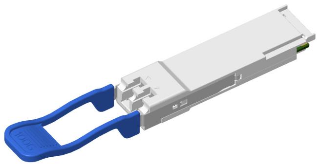
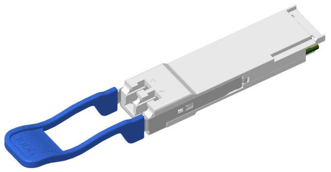
QSFP28 transceiver modules are designed for use in 100 Gigabit Ethernet links over single mode fiber.
They are compliant with SFF-8665, INF-8438i and IEEE 802.3ba 100GBASE-LR4. Digital diagnostics functions are available via an I2C interface, as specified by the QSFP28 MSA.
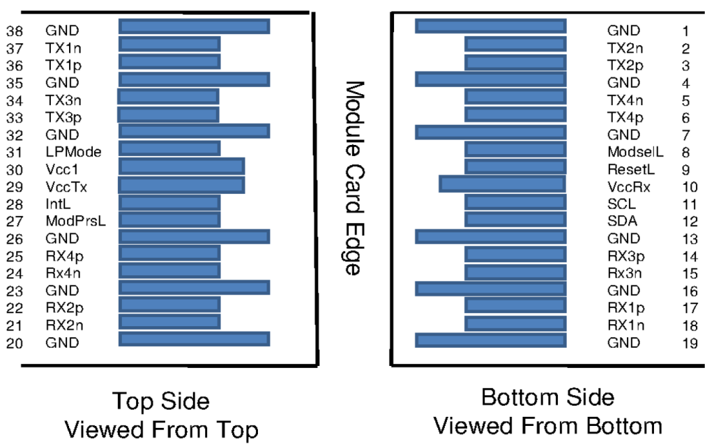
Pin function definitions
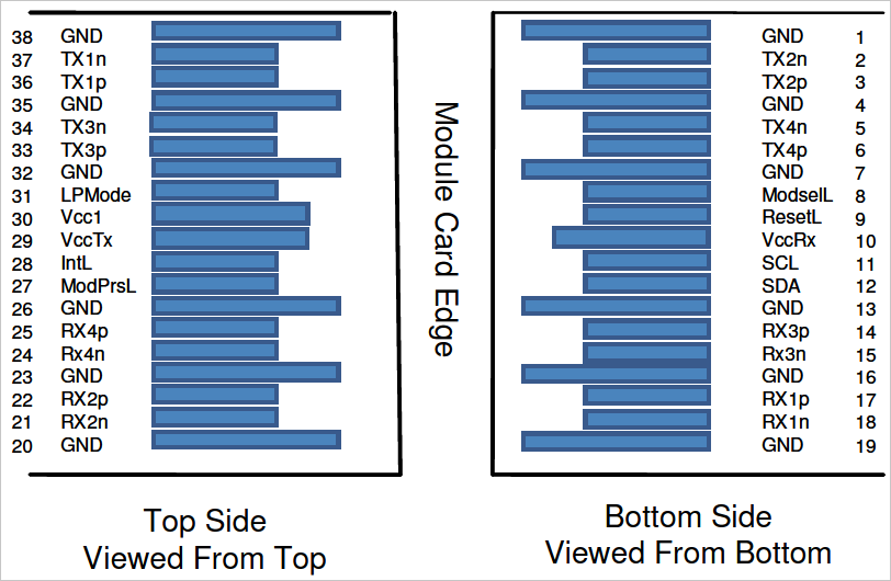
Figure 1.Pin function definitions
Table 1: Transceiver pin descriptions
|
Pin |
Name |
Description |
Plug Sequence |
Notes |
|
1 |
GND |
Ground |
1 |
|
|
2 |
Tx2n |
Transmitter Inverted Data Input |
3 |
|
|
3 |
Tx2p |
Transmitter Non-Inverted Data Input |
3 |
|
|
4 |
GND |
Ground |
1 |
|
|
5 |
Tx4n |
Transmitter Inverted Data Input |
3 |
|
|
6 |
Tx4p |
Transmitter Non-Inverted Data Input |
3 |
|
|
7 |
GND |
Ground |
1 |
|
|
8 |
ModSelL |
Module Select |
3 |
|
|
9 |
ResetL |
Module Reset |
3 |
|
|
10 |
Vcc Rx |
+3.3 V Power supply receiver |
2 |
|
|
11 |
SCL |
2-wire serial interface clock |
3 |
|
|
12 |
SDA |
2-wire serial interface data |
3 |
|
|
13 |
GND |
Ground |
1 |
|
|
14 |
Rx3p |
Receiver Non-Inverted Data Output |
3 |
|
|
15 |
Rx3n |
Receiver Inverted Data Output |
3 |
|
|
16 |
GND |
Ground |
1 |
|
|
17 |
Rx1p |
Receiver Non-Inverted Data Output |
3 |
|
|
18 |
Rx1n |
Receiver Inverted Data Output |
3 |
|
|
19 |
GND |
Ground |
1 |
|
|
20 |
GND |
Ground |
1 |
|
|
21 |
Rx2n |
Receiver Inverted Data Output |
3 |
|
|
22 |
Rx2p |
Receiver Non-Inverted Data Output |
3 |
|
|
23 |
GND |
Ground |
1 |
|
|
24 |
Rx4n |
Receiver Inverted Data Output |
3 |
|
|
25 |
Rx4p |
Receiver Non-Inverted Data Output |
3 |
|
|
26 |
GND |
Ground |
1 |
|
|
27 |
ModPrsL |
Module Present |
3 |
|
|
28 |
IntL |
Interrupt |
3 |
|
|
29 |
Vcc Tx |
+3.3 V Power supply transmitter |
2 |
|
|
30 |
Vcc1 |
+3.3 V Power Supply |
2 |
|
|
31 |
LPMode |
Low Power Mode |
3 |
|
|
32 |
GND |
Ground |
1 |
|
|
33 |
Tx3p |
Transmitter Non-Inverted Data Input |
3 |
|
|
34 |
Tx3n |
Transmitter Inverted Data Input |
3 |
|
|
35 |
GND |
Ground |
1 |
|
|
36 |
Tx1p |
Transmitter Non-Inverted Data Input |
3 |
|
|
37 |
Tx1n |
Transmitter Inverted Data Input |
3 |
|
|
38 |
GND |
Ground |
1 |
Absolute Maximum Ratings
|
Parameter |
Symbol |
Unit |
Min |
Max |
|
Storage Temperature Range |
Ts |
oC |
-40 |
85 |
|
Relative Humidity |
RH |
% |
0 |
95 |
|
Maximum Supply Voltage |
Vcc3 |
V |
-0.5 |
4.0 |
Recommended Operating Conditions
|
Parameter |
Symbol |
Unit |
Min |
Typ |
Max |
|
Operating Case Temperature Range |
Tc |
oC |
0 |
70 |
|
|
Power Supply Voltage |
Vcc |
V |
3.14 |
3.3 |
3.46 |
|
Bit Rate |
BR |
Gb/s |
103.1 |
||
|
Bit Error Ratio |
BER |
1E-12 |
|||
|
Max Supported Link Length |
L |
Km |
10 |
Electric Ports Definition
|
Parameter |
Symbol |
Unit |
Min |
Typ |
Max |
Note |
|
Supply Voltage |
VCC |
V |
3.14 |
3.3 |
3.46 |
|
|
Module Power |
mW |
4500 |
||||
|
Transmitter |
||||||
|
Input Differential Impedance |
RIN |
Ω |
10 |
100 |
110 |
|
|
Differential Data Input |
VIN |
mVp-p |
35 |
900 |
||
|
Differential input return loss (min) |
RLd |
dB |
IEEE 802.3ba, Section 83E-5 |
|||
|
Differential to common mode input return loss (min) |
RLdc |
dB |
IEEE 802.3ba, Section 83E-6 |
|||
|
Receiver |
||||||
|
Differential Data Output |
VOD |
mVp-p |
900 |
|||
|
AC common mode output voltage (RMS) |
mV |
17.5 |
||||
|
Differential output return loss (min) |
dB |
IEEE 802.3ba, Section 83E-2 |
||||
|
Differential to common mode input return loss (min) |
dB |
IEEE 802.3ba, Section 83E-2 |
||||
|
Output transition time,20% to80% |
ps |
12 |
||||
|
Vertical eye closure |
dB |
5.5 |
||||
Optical Characteristics (Tc=0 oC to 70 oC and Vcc= 3.14 to 3.46)
|
Parameter |
Symbol |
Unit |
Min |
Typ |
Max |
Notes |
|
Transmitter(per Lane) |
||||||
|
Signaling Speed per Lane |
GBd |
25.78125 ± 100 ppm |
||||
|
Lane Wavelength (range): L0 L1 L2 L3 |
nm |
1294.53 – 1296.59 1299.02 – 1301.09 1303.54 – 1305.63 1308.09 – 1310.19 |
||||
|
Total Average Launch Power |
Pout |
dBm |
10.5 |
1 |
||
|
Transmit OMA per Lane |
TxOMA |
dBm |
-1.3 |
4.5 |
1 |
|
|
Average Launch Power per Lane |
TXPx |
dBm |
-4.3 |
4.5 |
1 |
|
|
Optical Extinction Ratio |
ER |
dB |
4 |
2 |
||
|
Side-Mode Suppression Ratio (SMSR) |
SMSR |
dB |
30 |
|||
|
Average launch power of OFF transmitter, per lane |
dBm |
-30 |
||||
|
Relative Intensity Noise |
RIN |
dB/Hz |
-130 |
|||
|
Optical Return Loss Tolerance |
dB |
20 |
||||
|
Transmitter Reflectance |
dB |
-12 |
||||
|
Transmitter Eye mask definition {X1,X2,X3, Y1,Y2,Y3} |
{0.25,0.4,0.45,0.25,0.28,0.4} |
2 |
||||
|
Receiver(per Lane) |
||||||
|
Signaling Speed per Lane |
GBd |
25.78125 ± 100 ppm |
||||
|
Lane Wavelength (range): L0 L1 L2 L3 |
nm |
1294.53 – 1296.59 1299.02 – 1301.09 1303.54 – 1305.63 1308.09 – 1310.19 |
||||
|
Average Receiver Sensitivity per Lane |
Rxsens |
dBm |
-8.6 |
3 |
||
|
Average Received Power per Lane |
RXPx |
dBm |
-10.6 |
4.5 |
||
|
Damage Threshold Per Lane |
Pmax |
dBm |
5.5 |
|||
|
Return Loss |
RL |
-26 |
||||
|
Vertical eye closure penalty, per lane |
dB |
1.8 |
||||
|
Receiver electrical 3dB upper cutoff frequency,per lane |
GHz |
31 |
||||
|
LOS De-Assert |
LOSD |
dBm |
-13 |
|||
|
LOS Assert |
LOSA |
dBm |
-30 |
|||
|
LOS Hysteresis |
dB |
0.5 |
1.5 |
5 |
||
Note:
- The optical power is launched into SMF.
- Measured with a PRBS 231-1 test pattern @25.78125, Hit ratio≤5E-5.
- Measured with a PRBS 231-1 test pattern @25.78125 Gb/s, BER≤1E-12
Typical Application Circuit
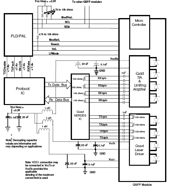
Figure 2. Typical application circuit
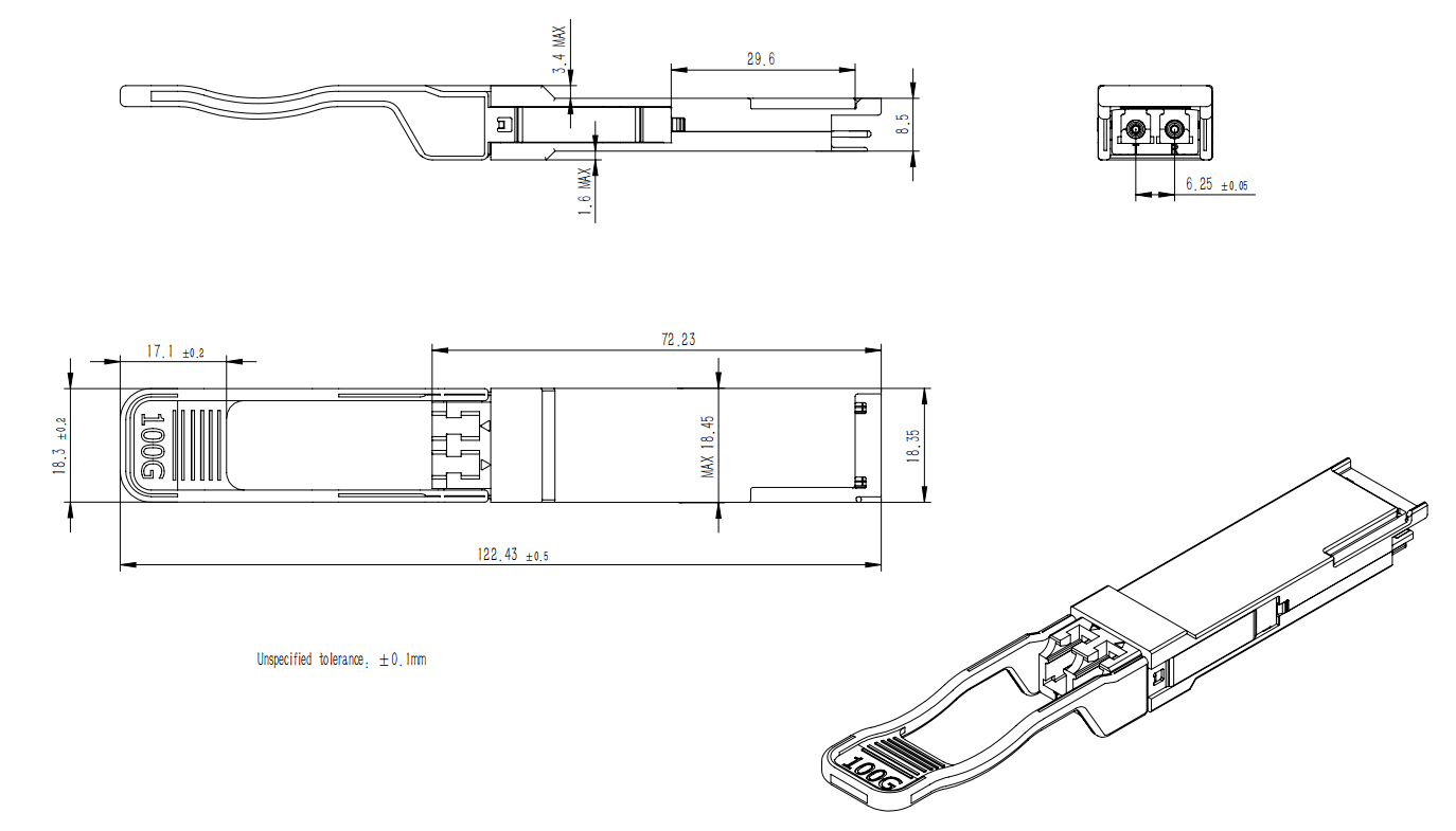
Mechanical Dimensions