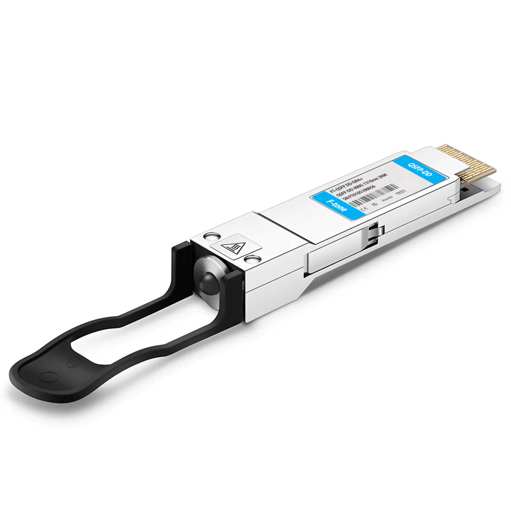
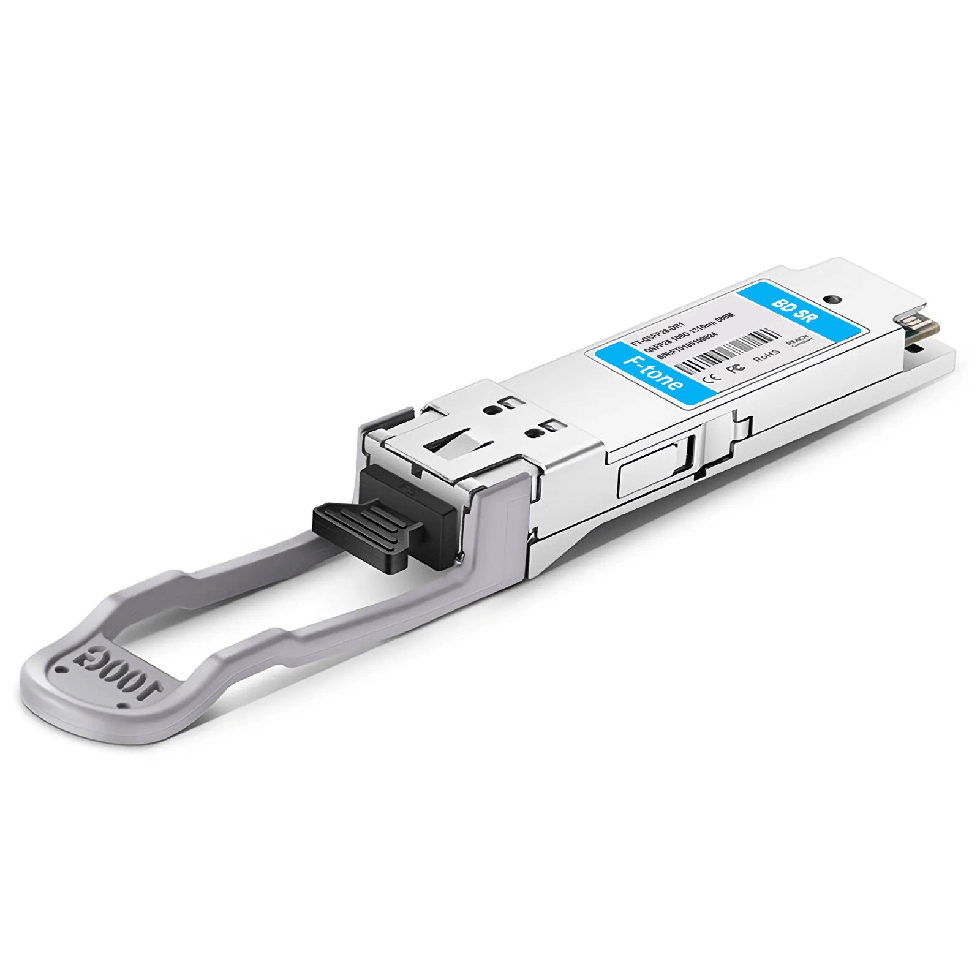
200GBASE-CWDM4 10KM QSFP56 Optical Transceiver Module
FTQ5-2H-CWDM4-10KM
Features
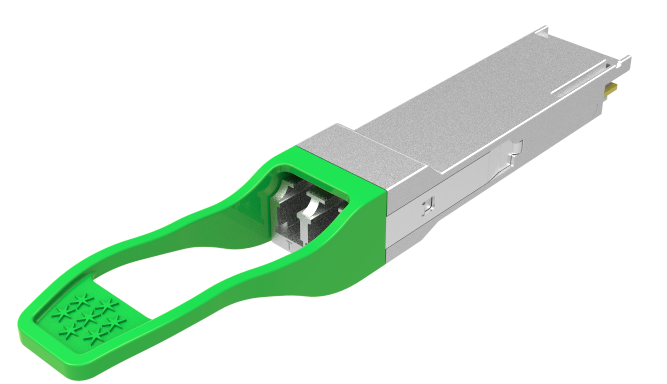
- Hot-pluggable QSFP56 form factor
- Built-in 200G PAM4 DSP
- Supports 212.5Gb/s aggregate bit rates
- Low power dissipation < 6W
- Commercial case temperature range of 0°C to 70°C
- Single 3.3V power supply
- Maximum link length of 10km on SMF
- 4 channels DML TOSA (uncooled)
- 4 channels PIN ROSA
- 4 CWDM lanes MUX/DEMUX design
- LC duplex connector
- 200GAUI-4 electrical interface
- Compliant with CMIS 4.0
- I2C management interface
- Built-in digital diagnostic functionality
- RoHS compliant and lead free
Applications
- 200GBASE-FR4 Ethernet (PAM4)
- Data Center Network
Description
F-tone Networks’s FTQ5-2H-CWDM4-10KM Optical Transceiver modules are designed for use in 200 Gigabit Ethernet links over single-mode fiber. The module can convert 4-channel 53.125 Gbps electrical data to 4-channel optical signals, and multiplex them into a single channel for 212.5 Gbps optical transmission. Similarly, it optically de-multiplexes a 212.5 Gbps input into 4-channel signals, and converts them to 4-channel output electrical data on the receiver side.
They are compliant with the QSFP+ MSA and with IEEE 802.3cn 200GBASE, SFF-8679, and CEI-56G-VSR-PAM4 standards. Digital diagnostics functions are available via the I2C interface as specified by CMIS4.0. The transceiver is RoHS 2.0 compliant and lead-free per Directive 2011/65/EU.
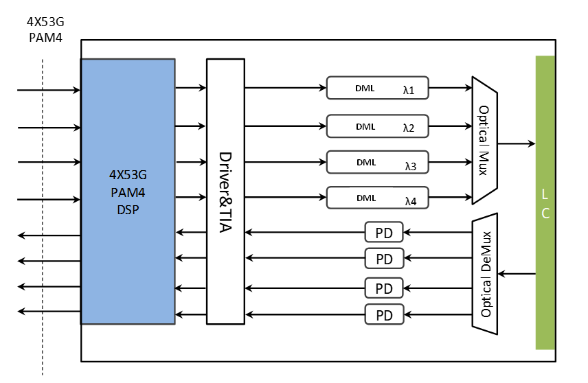
Figure 1. Module Block Diagram
Absolute Maximum Ratings
|
Parameter |
Symbol |
Min |
Max |
Unit |
|
Supply Voltage |
Vcc |
-0.3 |
3.6 |
V |
|
Input Voltage |
Vin |
-0.3 |
Vcc+0.3 |
V |
|
Storage Temperature |
Ts |
-20 |
85 |
ºC |
|
Case Operating Temperature |
Tc |
0 |
70 |
ºC |
|
Humidity (non-condensing) |
Rh |
5 |
95 |
% |
Recommended Operating Conditions
|
Parameter |
Symbol |
Min |
Typical |
Max |
Unit |
|
Supply Voltage |
Vcc |
3.13 |
3.3 |
3.47 |
V |
|
Operating Case Temperature |
Tc |
0 |
70 |
ºC |
|
|
Baud Rate per Lane (PAM4) |
fd |
26.5625 |
GBaud/s |
||
|
Humidity |
Rh |
5 |
85 |
% |
|
|
Power Dissipation |
Pm |
6.0 |
W |
Electrical Specifications
|
Parameter |
Symbol |
Min |
Typical |
Max |
Unit |
|
Differential Input Impedance |
Zin |
90 |
100 |
110 |
ohm |
|
Differential Output Impedance |
Zout |
90 |
100 |
110 |
ohm |
|
Differential Input Voltage Amplitude |
ΔVin |
300 |
900 |
mVpp |
|
|
Differential Output Voltage Amplitude |
ΔVout |
300 |
900 |
mVpp |
|
|
Bit Error Rate |
BER |
2.4E-4 |
|||
|
Input Logic Level High |
VIH |
2.0 |
Vcc |
V |
|
|
Input Logic Level Low |
VIL |
0 |
0.8 |
V |
|
|
Output Logic Level High |
VOH |
Vcc-0.5 |
Vcc |
V |
|
|
Output Logic Level Low |
VOL |
0 |
0.4 |
V |
Optical Characteristics
|
Parameter |
Symbol |
Min |
Typical |
Max |
Unit |
|
|
Transmitter |
||||||
|
Center Wavelength |
L1 |
1264.5 |
1277.5 |
nm |
||
|
Center Wavelength |
L2 |
1284.5 |
1297.5 |
nm |
||
|
Center Wavelength |
L3 |
1304.5 |
1317.5 |
nm |
||
|
Center Wavelength |
L4 |
1324.5 |
1337.5 |
nm |
||
|
SMSR |
SMSR |
30 |
nm |
|||
|
Average Launch Power (each lane) |
Pout |
-4.2 |
4.7 |
dBm |
||
|
Average Launch Power (total) |
Ptatal |
10.7 |
dBm |
|||
|
Outer Optical Modulation Amplitude (each lane) |
OMAout |
-1.2 |
4.5 |
dBm |
||
|
Difference in launch power between any two lanes (OMAouter) |
DOMA |
4 |
dB |
|||
|
Transmitter and dispersion eye closure (each lane) |
TDECQ |
3.1 |
dB |
|||
|
Average launch power of off transmitter (each lane) |
Poff |
-30 |
dBm |
|||
|
Outer Extinction Ratio |
ER |
3.5 |
dB |
|||
|
Optical Return Loss Tolerance |
ORLT |
17.1 |
dB |
|||
|
Receiver |
||||||
|
Center Wavelength |
L1 |
1264.5 |
1277.5 |
nm |
||
|
Center Wavelength |
L2 |
1284.5 |
1297.5 |
nm |
||
|
Center Wavelength |
L3 |
1304.5 |
1317.5 |
nm |
||
|
Center Wavelength |
L4 |
1324.5 |
1337.5 |
nm |
||
|
Damage threshold |
Rdam |
5.7 |
dBm |
|||
|
Average Receive Power (each lane) Input (each lane) |
Pin |
-8.2 |
4.7 |
dBm |
||
|
Receiver Power (OMAouter) (each lane) |
OMAout |
4.5 |
dBm |
|||
|
Receiver reflectance |
Pref |
-26 |
dB |
|||
|
Stressed Receiver Sensitivity(OMAouter) (each lane) |
Sens |
-3.8 |
dBm |
|||
|
Receiver Sensitivity (OMAouter) (each lane) Note1 |
Sen |
max (-5.5, SECQ-6.9) |
dBm |
|||
Note:
- Note1. Measured with conformance test signal at TP3 for the BER specified in IEEE 802.3cn.
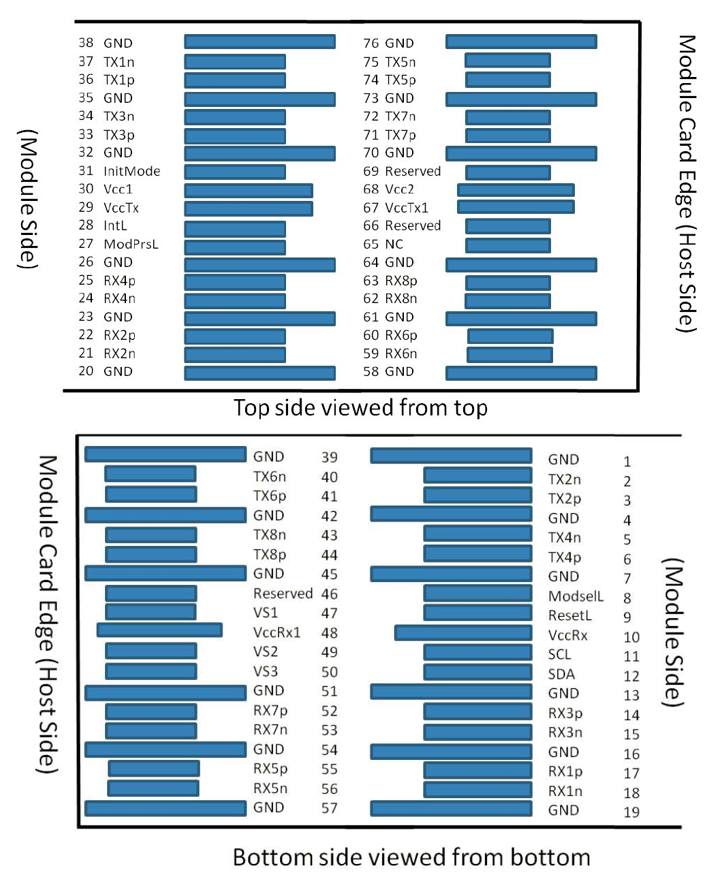
Pin Description
|
Logic |
Symbol |
Name/Description |
|
|
1 |
GND |
Module GroundNote2 |
|
|
2 |
CML-I |
Tx2- |
Transmitter inverted data input |
|
3 |
CML-I |
Tx2+ |
Transmitter non-inverted data input |
|
4 |
GND |
Module Ground Note2 |
|
|
5 |
CML-I |
Tx4- |
Transmitter inverted data input |
|
6 |
CML-I |
Tx4+ |
Transmitter non-inverted data input |
|
7 |
GND |
Module GroundNote2 |
|
|
8 |
LVTTL-I |
MODSEIL |
Module SelectNote3 |
|
9 |
LVTTL-I |
ResetL |
Module ResetNote3 |
|
10 |
VCCRx |
+3.3V Receiver Power Supply |
|
|
Pin |
Logic |
Symbol |
Name/Description |
|
11 |
LVCMOS-I |
SCL |
2-wire Serial interface clockNote3 |
|
12 |
LVCMOS-I/O |
SDA |
2-wire Serial interface dataNote3 |
|
13 |
GND |
Module GroundNote2 |
|
|
14 |
CML-O |
RX3+ |
Receiver non-inverted data output |
|
15 |
CML-O |
RX3- |
Receiver inverted data output |
|
16 |
GND |
Module GroundNote2 |
|
|
17 |
CML-O |
RX1+ |
Receiver non-inverted data output |
|
18 |
CML-O |
RX1- |
Receiver inverted data output |
|
19 |
GND |
Module GroundNote2 |
|
|
20 |
GND |
Module GroundNote2 |
|
|
21 |
CML-O |
RX2- |
Receiver inverted data output |
|
22 |
CML-O |
RX2+ |
Receiver non-inverted data output |
|
23 |
GND |
Module GroundNote2 |
|
|
24 |
CML-O |
RX4- |
Receiver inverted data output |
|
25 |
CML-O |
RX4+ |
Receiver non-inverted data output |
|
26 |
GND |
Module GroundNote2 |
|
|
27 |
LVTTL-O |
ModPrsL |
Module Present, internal pulled down to GND |
|
28 |
LVTTL-O |
IntL |
Interrupt output, should be pulled up on host board |
|
29 |
VCCTx |
+3.3V Transmitter Power Supply |
|
|
30 |
VCC1 |
+3.3V Power Supply |
|
|
31 |
LVTTL-I |
LPMode |
Low Power ModeNote3 |
|
32 |
GND |
Module GroundNote2 |
|
|
33 |
CML-I |
Tx3+ |
Transmitter non-inverted data input |
|
34 |