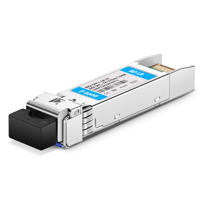
FTCS-B271X-40D 10Gb/s 40Km SFP+ BiDi Transceiver
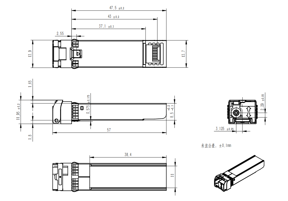
The FTCS-B271X-40D is a 10Gb/s 40km SFP+ BiDi (Bidirectional) transceiver compliant with SFP+ MSA. Features 1270nm/1330nm laser, LC single connector, hot pluggable 20-pin interface, low power consumption <1W, and digital diagnostics (SFF-8472).
10Gb/s 40Km SFP+ BIDI Transceivers
FTCS-B271X-40D
Features
- Compliant to SFP+ MSA
- Fully RoHS Compliant
- All metal housing for superior EMI performance
- Operating data rate up to 11.3Gbps
- 1270nm/1330nm Laser
- High sensitivity Pin photodiode and TIA
- LC single connector
- Hot pluggable 20pin connector
- Low power consumption <1W
- 0℃ to 70℃ operating wide temperature range
- Single +3.3V±5% power supply
- Digital Monitoring SFF-8472 Rev 10.2 compliant
Applications
- 10GBASE-LR/LW
- 10G Fiber Channel
- SFP+ MSA (SFF-8472)
- IEEE802.3ae
The laser based 10Gigabit SFP+ Transceiver is designed to transmit and receive serial optical data over single mode optical fiber with 40Km.
They are compliant with SFF-8431,SFF-8432, 10GFC Rev 4.0,. The transmitter converts serial CML electrical data into serial optical data compliant with the IEEE 802.3ae standard. The receiver converts serial optical data into serial CML electrical data.Digital diagnostics functions are available via a 2-wire serial interface, as specified in SFF-8472.
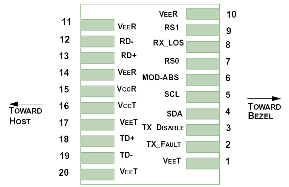
Pin function definitions
Figure 1.Pin function definitions
Table 1: Transceiver pin descriptions
|
Pin Number |
Symbol |
Name |
Description |
|
1,17,20 |
VeeT |
Transmitter Signal Ground |
These pins should be connected to signal ground on the host board. |
|
2 |
TX Fault |
Transmitter Fault Out (OC) |
Logic “1” Output = Laser Fault (Laser off before t_fault) Logic “0” Output = Normal Operation This pin is open collector compatible, and should be pulled up to Host Vcc with a 10kΩ resistor. |
|
3 |
TX Disable |
Transmitter Disable In (LVTTL) |
Logic “1” Input (or no connection) = Laser off Logic “0” Input = Laser on This pin is internally pulled up to VccT with a 10 kΩ resistor. |
|
4 |
SDA |
Module Definition Identifiers |
Serial ID with SFF 8472 Diagnostics Module Definition pins should be pulled up to Host Vcc with 10 kΩ resistors. |
|
5 |
SCL |
||
|
6 |
MOD-ABS |
||
|
7 |
RS0 |
Receiver Rate Select (LVTTL) Transmitter Rate Select (LVTTL) |
These pins have an internal 30kΩ pull-down to ground. A signal on either of these pins will not affect module performance. |
|
9 |
RS1 |
||
|
8 |
LOS |
Loss of Signal Out (OC) |
Sufficient optical signal for potential BER < 1×10-12 = Logic “0” Insufficient optical signal for potential BER < 1×10-12 = Logic “1” This pin is open collector compatible, and should be pulled up to Host Vcc with a 10kΩ resistor. |
|
10,11,14 |
VeeR |
Receiver Signal Ground |
These pins should be connected to signal ground on the host board. |
|
12 |
RD- |
Receiver Negative DATA Out (CML) |
Light on = Logic “0” Output Receiver DATA output is internally AC coupled and series terminated with a 50Ω resistor. |
|
13 |
RD+ |
Receiver Positive DATA Out (CML) |
Light on = Logic “1” Output Receiver DATA output is internally AC coupled and series terminated with a 50Ω resistor. |
|
15 |
VccR |
Receiver Power Supply |
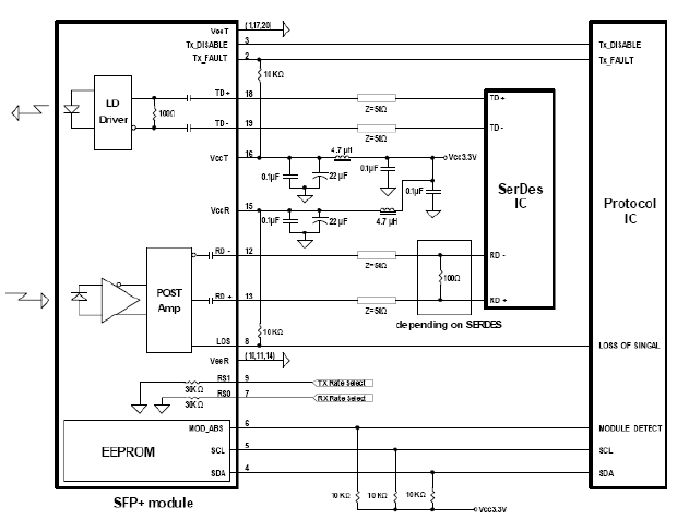
This pin should be connected to a filtered +3.3V power supply on the host board. See Figure 3.Recommended power supply filter |
|
16 |
VccT |
Transmitter Power Supply |
This pin should be connected to a filtered +3.3V power supply on the host board. See Figure 3.Recommended power supply filter |
|
18 |
TD+ |
Transmitter Positive DATA In (CML) |
Logic “1” Input = Light on Transmitter DATA inputs are internally AC coupled and terminated with a differential 100Ω resistor. |
|
19 |
TD- |
Transmitter Negative DATA In (CML) |
Logic “0” Input = Light on Transmitter DATA inputs are internally AC coupled and terminated with a differential 100Ω resistor. |
Absolute Maximum Ratings
|
Parameter |
Symbol |
Unit |
Min |
Max |
|
Storage Temperature Range |
Ts |
oC |
-40 |
85 |
|
Relative Humidity |
RH |
% |
0 |
95 |
|
Maximum Supply Voltage |
Vcc3 |
V |
-0.5 |
3.6 |
General Specifications
|
Parameter |
Symbol |
Min |
Typ |
Max |
Units |
Ref. |
|
Bit Rate |
BR |
11.3 |
Gb/s |
1 |
||
|
Bit Error Ratio |
BER |
10E-12 |
2 |
|||
|
Max. Supported Link Length |
LMAX |
40 |
km |
1 |
Notes:
1. 10GBASE-LR, 10GBASE-LW, 1200-SM-LL-L 10GFC.
2. Tested with a 231-1 PRBS.
Recommended Operating Conditions
|
Parameter |
Symbol |
Unit |
Min |
Typ |
Max |
|
Operating Case Temperature Range |
Tc |
oC |
0 |
70 |
|
|
Power Supply Voltage |
Vcc |
V |
3.14 |
3.3 |
3.46 |
|
Bit Rate |
BR |
Gb/s |
11.3 |
||
|
Bit Error Ratio |
BER |
10-12 |
|||
|
Max Supported Link Length |
L |
Km |
40 |
Electric Ports Definition
|
Parameter |
Symbol |
Unit |
Min |
Typ |
Max |
Note |
|
Supply Voltage |
VCC |
V |
3.14 |
3.3 |
3.46 |
|
|
Module Power |
Icc |
mW |
1000 |
|||
|
Transmitter |
||||||
|
Input Differential Impedance |
RIN |
Ω |
80 |
100 |
120 |
|
|
Differential Data Input |
VIN |
mVp-p |
180 |
700 |
||
|
Transmit Disable Voltage |
VDIS |
V |
2 |
VCCHOST |
||
|
Transmit Enable Voltage |
VEN |
V |
VEE |
VEE+0.8 |
||
|
Transmit Fault Assert Voltage |
VFA |
V |
2 |
VCCHOST |
||
|
Transmit Fault De-Assert Voltage |
VFDA |
V |
VEE |
VEE+0.4 |
||
|
Receiver |
||||||
|
Differential Data Output |
VOD |
mVp-p |
300 |
850 |
||
|
Output Rise Time |
tRISE |
pS |
25 |
|||
|
Output Fall Time |
tFALL |
pS |
25 |
|||
|
LOS Fault |
VLOSFT |
V |
2 |
VCCHOST |
||
|
LOS Normal |
VLOSNR |
V |
VEE |
VEE+0.4 |
||
|
Parameter |
Symbol |
Min |
Typ |
Max |
Note |
Unit |
|
Optical Transmitter Characteristics |
||||||
|
Nominal Wavelength (FLS10C411S) |
λC |
1260 |
1270 |
1280 |
nm |
|
|
Nominal Wavelength (FLS10C412S) |
λC |
1320 |
1330 |
1340 |
nm |
|
|
Optical Output Power |
Pav |
1 |
5 |
dBm 本产品为10G SFP+ BiDi Transceiver产品线,详细信息,请联系我们的销售人员,谢谢! Important Notice 公司名:北亿纤通| F-toneNetworks | ||