FTQ2-HG-LX4 100Gb/s QSFP28 LX4 MMF/SMF 1310nm 100m/2km Optical Transceiver
Features
- Four-channel full-duplex transceiver modules
- Transmission data rate up to 26Gbit/s per channel
- Up to 100m transmission on OM3 multimode fiber (MMF) or 2km transmission on single mode fiber (SMF)
- Low power consumption <4W
- Operating case temperature 0°C to +70°C
- 3.3V power supply voltage
- RoHS compliant
- Hot Pluggable QSFP28 form factor
- LC connector receptacle
- Built-in digital diagnostic function
Applications
- 100G Ethernet
- Proprietary High Speed Interconnections
- Datacenter
- 100G LX4 application with FEC
Description
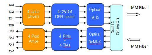
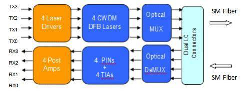
This product is a transceiver module designed for optical transmission applications over both MMF and SMF with transmission distances of up to 100m on MMF (OM3) and 2km on SMF. The module converts 4 inputs channels (ch) of 25Gb/s electrical data to 4 CWDM optical signals, and multiplexes them into a single channel for 100Gb/s optical transmission.
Reversely, on the receiver side, the module optically de-multiplexes a 100Gb/s input into 4 CWDM channels signals, and converts them to 4 channel output electrical data.
The central wavelengths of the 4 CWDM channels are 1271, 1291, 1311 and 1331nm as members of the CWDM wavelength grid defined in ITU-T G.694.2. It contains a duplex LC connector for the optical interface and a 38-pin connector for the electrical interface.
The product is designed with form factor, optical/electrical connection and digital diagnostic interface according to the QSFP28 Multi-Source Agreement (MSA). It has been designed to meet the harshest external operating conditions including temperature, humidity and EMI interference.
For applications over OM3/OM4 MMF, MMF cables are directly connected to the LC connectors of QSFP28 LX4 module and optical signal is directly launched from the transmitter into the MMF cable as shown in Figure 2. For applications over SMF, the module is used as a QSFP28 CWDM4 module and SMF cables are directly connected to the LC connectors of the module as shown in Figure 3.
Table 1 – Absolute Maximum Ratings
| Symbols | Min. | Max. | Unit | Notes |
|---|---|---|---|---|
| TS | -40 | 85 | ℃ | |
| ure TOP | 0 | 70 | ℃ | |
| VCC | -0.5 | 3.6 | V | |
| RH | 0 | 85 | % | |
| ane THd | 4.5 | dBm |
Table 2 – Recommended Operating Conditions and Power Supply Requirements
| Table2-Recommended Operating Conditions and Power Supply Requirements | ||||||
|---|---|---|---|---|---|---|
| Parameter | Symbols | Min. | Typical | Max. | Unit | Notes |
| Operating Case Temperatu | re TOP | 0 | 70 | ℃ | ||
| Power Supply Voltage | VCC | 3.135 | 3.3 | 3.465 | V | |
| Data Rate, each Lane | 25.78125 | Gb/s | ||||
| Control Input Voltage Hig | h | 2 | VCC | V | ||
| Control Input Voltage Lo | w | 0 | 0.8 | V | ||
| Link Distance(OM3MMF | ) D_MMF | 100 | m | |||
| Link Distance(SMF) | D_SMF | 2 | km |
Table 3 – Electrical Characteristics
| Table3-Electrical C haracteristics | ||||||
|---|---|---|---|---|---|---|
| Parameter | TestPoint | Min. | Typical | Max. | Unit | Notes |
| Power Consumption | 4 | W | ||||
| Supply Current | ICC | 1.22 | A | |||
| Transceiver Power-on Initialization Time |
2000 | ms | 1 | |||
| Transmitter(each Lane) | ||||||
| Single-ended Input Voltage Tolerance(Note2) |
-0.3 | 4.0 | V | Referredto TP1 signal common |
||
| AC Common Mode Input Voltage Tolerance |
15 | mV | RMS | |||
| Differential Input Voltage SwingThreshold |
50 | mVpp | LOSA Threshold |
|||
| Differential Input Voltage Swing |
Vin,pp | 190 | 700 | mVpp | ||
| Differential Input Impedanc | e Zin | 90 | 100 | 110 | ohm | |
| Differential Input Return Lo | ss | SeeIEEE802.3ba86A.4.11 | dB | 10MHz-11. 1GHz |
||
| J2 Jitter Tolerance | Jt2 | 0.17 | UI | |||
| J9 Jitter Tolerance | Jt9 | 0.29 | UI | |||
| Data Dependent Pulse Widt Shrinkage(DDPWS)Toleranc |
h e |
0.07 | UI | |||
| Eye Mask Coordinates{X1,X Y1,Y2} |
2, | 0.11,0.31 95,350 |
UI mV |
HitRatio= 5×10⁻⁵ |
||
| Receiver(each Lane) | ||||||
| Single-ended Output Voltag | e | -0.3 | 4.0 | V | Referredto signal common |
|
| AC Common Mode Output Voltage |
7.5 | mV | RMS | |||
| Differential Output Voltage Swing |
Vout,pp | 300 | 850 | mVpp | ||
| Differential Out put Impedance |
Zout | 90 | 100 | 110 | ohm | |
| Termination Mismatchat 1 MHz |
5 | % | ||||
| Differential Out put Return Loss |
SeeIEEE 802.3ba 86A.4.2.1 | dB | 10MHz- |
| 11.1GHz | ||||||
|---|---|---|---|---|---|---|
| Common Mode Output Retur Loss |
n | SeeIEEE802.3ba86A.4.2.2 | dB | 10MHz-11. 1GHz |
||
| Output Transition Time | 28 | Ps | 20%to80% | |||
| J2 Jitter Output | Jo2 | 0.42 | UI | |||
| J9 Jitter Output | Jo9 | 0.65 | UI | |||
| Eye Mask Coordinates{X1,X2, ,Y2} |
Y1 | 0.29,0.5,150,425 | UI mV |
HitRatio= 5×10⁻⁵ |
Notes:
[1] Power-on Initialization Time is the time from when the power supply voltages reach and remain above the minimum recommended operating supply voltages to the time when the module is fully functional.
[2] The single ended input voltage tolerance is the allowable range of the instantaneous input signals.
Table 4 – Optical Characteristics
| Table4-Optical Characteristics | ||||||
|---|---|---|---|---|---|---|
| Parameter | Symbols | Min. | Typical | Max. | Unit | Notes |
| Wavelength Assignment | L0 L1 L2 L3 |
1264.5 | 1271 | 1277.5 | nm | |
| 1284.5 | 1291 | 1297.5 | nm | |||
| 1304.5 | 1311 | 1317.5 | nm | |||
| 1324.5 | 1331 | 1337.5 | nm | |||
| Transmitter | ||||||
| Total Average Launch Power (forSMF) |
PT,SMF | 8.3 | dBm | |||
| Total Average Launch Power (forMMF) |
PTMMF , |
9.5 | dBm | |||
| Average Launch Power,each Lane(forSMF) |
PAVG,SMF | -6.5 | 2.5 | dBm | ||
| Average Launch Power,each Lane(forMMF) |
PAVG,MMF | -4.5 | 4.5 | dBm | ||
| Optical Modulation Amplitud (OMA), each Lane(forSMF) |
e POMA,SMF |
-4.5 | 2.5 | dBm | 1 | |
| Optical Modulation Amplitud (OMA), each Lane(forMMF) |
e POMA,MMF |
-3 | 4.5 | dBm | ||
| Differencein Launch Power between any Two Lanes(OM |
Ptx,diff A |
6.5 | dB | |||
| ) Launch Power in OMA minu Transmitter and Dispersion Penalty(TDP) each Lane |
s , |
-6.8 | dBm | |||
| TDP,each Lane | TDP | 2.6 | dB | |||
| Extinction Ratio | ER | 3.5 | dB |
| RelativeIntensity Noise | RIN | -128 | dB/Hz | 12dB reflection |
||
|---|---|---|---|---|---|---|
| Transmitter Reflectance | RT | -12 | dB | |||
| Average Launch Power OFF Transmitter, each Lane |
Poff | -30 | dBm | |||
| Receive r | ||||||
| Overload power, each Lane (AVG) |
4.5 | dBm | 2 | |||
| Total Average Receive Pow (for SMF) |
er | 8.3 | dBm | |||
| Total Average Receive Pow (forMMF) |
er | 9.5 | dBm | |||
| Average Receive Power, each Lane(forSMF) |
-11.5 | 4.5 | dBm | |||
| Average Receive Power, each Lane(forMMF) |
-8 | 3.5 | dBm | |||
| Receiver Reflectance | RR | -26 | dB | |||
| Receiver Sensitivity (OMA) each Lane(forSMF) |
, SEN,SMF |
-11.5 | dBm | 3 | ||
| Receiver Sensitivity(OMA), each Lane(for MMF) |
SEN,MMF | -8 | dBm | 3 | ||
| Difference in Receive Powe between any Two Lanes(OMA) |
r Prx,diff |
7.5 | dB | |||
| LOS Assert | LOSA | -28 | dBm | |||
| LOS Deassert | LOSD | -15 | dBm | |||
| LOS Hysteresis | LOSH | 0.5 | dB | |||
| Receiver Electrical 3dB upperCut off Frequency, each Lane |
FC | 12.3 | GHz |
Notes:
[1] Even if the TDP<0.8dB, the OMA min must exceed the minimum value specified here.
[2] The receiver shall be able to tolerate, without damage, continuous exposure to a modulated optical input signal having this power level on one lane. The receiver does not have to operate correctly at this input power.
[3] Sensitivity is specified at 5×10⁻⁵ BER.
Table 5 – Digital Diagnostic Functions
| Table5-Digital Diagnostic Functions | |||||
|---|---|---|---|---|---|
| Parameter | Symbols | Min. | Max. | Unit | Notes |
| Temper aturemonit or absolute error |
DMI_Temp | -3 | +3 | ℃ | Overoperating temperature range |
| Supply voltagemonit or absolute error |
DMI_VCC | -0.1 | +0.1 | V | Over full operating range |
Pin Description
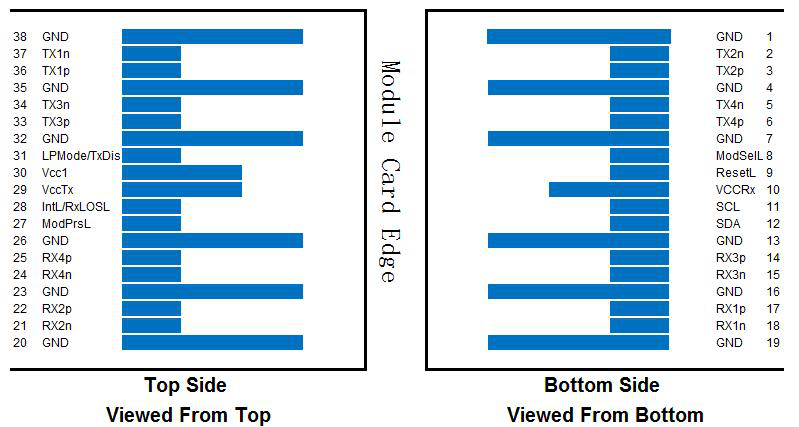
Table 6 – Pin Function Definitions
| Table6-Pin Function Definitions | |||
|---|---|---|---|
| Pin | Symbols | Description | Notes |
| 1 | GND | Ground | 1 |
| 2 | Tx2n | Transmitter Inverted Data Input | |
| 3 | Tx2p | Transmitter Non-Inverted Data Input | |
| 4 | GND | Ground | 1 |
| 5 | Tx4n | Transmitter Inverted Data Input | |
| 6 | Tx4p | Transmitter Non-Inverted Data Input | |
| 7 | GND | Ground | |
| 8 | ModSelL | Module Select | |
| 9 | ResetL | Module Reset | |
| 10 | VccRx | +3.3V Power Supply Receiver | 2 |
| 11 | SCL | 2-wire serial interface clock |
| 12 | SDA | 2-wire serial interface data | |
|---|---|---|---|
| 13 | GND | Ground | |
| 14 | Rx3p | Receiver Non-Inverted Data Output | |
| 15 | Rx3n | Receiver Inverted Data Output | |
| 16 | GND | Ground | 1 |
| 17 | Rx1p | Receiver Non-Inverted Data Output | |
| 18 | Rx1n | Receiver Inverted Data Output | 1 |
| 19 | GND | Ground | 1 |
| 20 | GND | Ground | |
| 21 | Rx2n | Receiver Inverted Data Output | |
| 22 | Rx2p | Receiver Non-Inverted Data Output | |
| 23 | GND | Ground | |
| 24 | Rx4n | Receiver Inverted Data Output | |
| 25 | Rx4p | Receiver Non-Inverted Data Output | |
| 26 | GND | Ground | 1 |
| 27 | ModPrsL | Module Present | |
| 28 | IntL | Interrupt | |
| 29 | VccTx | +3.3V Power supply transmitter | 2 |
| 30 | Vcc1 | +3.3V Power supply | 2 |
| 31 | LPMode | LowPowerMode | |
| 32 | GND | Ground | 1 |
| 33 | Tx3p | Transmitter Non-Inverted Data Input | |
| 34 | Tx3n | Transmitter Inverted Data Input | |
| 35 | GND | Ground | 1 |
| 36 | Tx1p | Transmitter Non-Inverted Data Input | |
| 37 | Tx1n | Transmitter Inverted Data Input | |
| 38 | GND | Ground | 1 |
Notes:
[1] GND is the symbol for signal and supply (power) common for the module. All are common within the module and all module voltages are referenced to this potential unless otherwise noted. Connect these directly to the host board signal-common ground plane.
[2] VccRx, Vcc1 and VccTx are the receiver and transmitter power supplies and shall be applied concurrently. Recommended host board power supply filtering is shown in Figure 2. Vcc Rx Vcc1 and Vcc Tx may be internally connected within the Module in any combination. The connector pins are each rated for a maximum current of 1000mA.
Block Diagram of Transceiver
Mechanical Dimensions
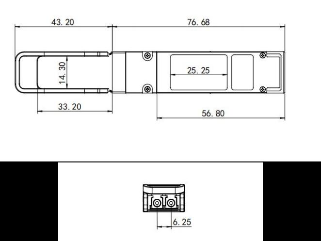
ESD
This transceiver is specified as ESD threshold 1kV for high speed data pins and 2kV for all other electrical input pins, tested per MIL-STD-883, Method 3015.4/JESD22-A114-A (HBM). However, normal ESD precautions are still required during the handling of this module. This transceiver is shipped in ESD protective packaging. It should be removed from the packaging and handled only in an ESD protected environment.
Laser Safety
This is a Class 1 Laser Product according to EN 60825-1:2014. This product complies with 21 CFR 1040.10 and 1040.11 except for deviations pursuant to Laser Notice No. 50, dated (June 24, 2007).
Caution: Use of controls or adjustments or performance of procedures other than those specified herein may result in hazardous radiation exposure.
Ordering Information
| Part Number | Product Description |
|---|---|
| FTQ2-HG-LX4 | QSFP28, 100Gb/s, LX4, 0℃ to+70℃ |
企业信息
| 项目 | 信息 |
|---|---|
| 公司名 | 北亿纤通 | F-toneNetworks |
| 地区 | 中国四川天府新区 |
| 服务区域 | 全球 |
| 企业电话 | 028-85255257 |
| 企业传真 | 028-85977702 |
| 企业手机 | 19081343401 |
| Site | https://www.f-tone.com |
| 人事部 | hr@f-tone.com |
| 市场部 | sales@f-tone.com |
| 技术支持 | support@f-tone.com |
本产品为100G QSFP28 LX4光收发模块产品线,详细信息,请联系我们的销售人员,谢谢!
Important Notice
Performance figures, data and any illustrative material provided in this data sheet are typical and must be specifically confirmed in writing by F-tone Networks before they become applicable to any particular order or contract. In accordance with the F-tone Networks policy of continuous improvement specifications may change without notice.
The publication of information in this data sheet does not imply freedom from patent or other protective rights of F-tone Networks or others. Further details are available from any F-tone Networks sales representative.