
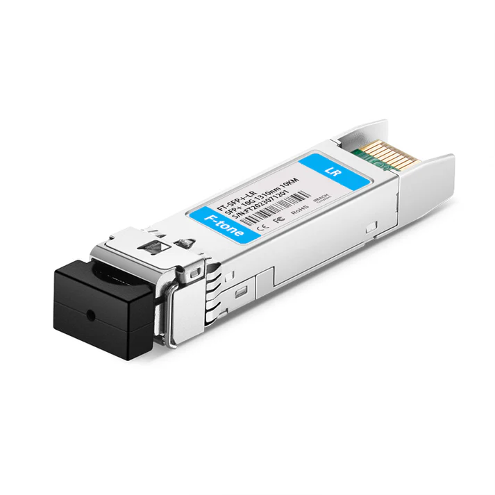
Product Overview / 产品简介
BYCS-131X-10Dxx 系列是北亿纤通(F-tone Networks)推出的 10G SFP+ 1310nm DUAL 10km 光收发器模块。该模块采用 1310nm DFB 激光器发射器和 PIN 光电探测器接收器,设计用于在单模光纤上传输和接收 10Gbit/s 串行光数据,最大传输距离 10km,符合 IEEE 802.3ae 10GBASE-LR 标准。
模块电气接口符合 SFF-8431 规范(增强型 8.5G/10G 小型可插拔模块”SFP+”),支持 SFF-8472 数字诊断监测接口(DDM),可实时监测温度、光功率、偏置电流和供电电压。提供商业级(0~70°C)和工业级(-40~85°C)两种工作温度版本,全金属外壳设计提供优异的 EMI 性能。
Product Features / 产品特点
- 10Gb/s 串行光接口,符合 802.3ae 10GBASE-LR 标准
- 电气接口符合 SFF-8431 规范(增强型 SFP+)
- 1310nm DFB 激光器发射器,PIN 光电探测器接收器
- 2-wire 管理接口,符合 SFF-8472 规范
- 数字诊断监测接口(DDM),支持光收发器实时监测
- 全金属外壳,优异的 EMI 性能
- 低功耗设计
- 高级固件支持客户系统加密信息存储于收发器中
- 高性价比 SFP+ 方案,支持更高端口密度和更大带宽
- RoHS 认证
- 工作温度:商业级 0~70°C / 工业级 -40~85°C
Applications / 应用场景
- 高速存储区域网络(SAN)
- 计算机集群交叉连接
- 定制高速数据管道
- 数据中心互连
- 企业级城域网
Description / 详细描述
该 1310nm DFB 10Gigabit SFP+ 收发器设计用于在单模光纤上传输和接收光数据,链路长度可达 10km。
SFP+ LR 模块电气接口符合 SFI 电气规范。发射器输入和接收器输出阻抗为 100 Ohm 差分。数据线内部 AC 耦合。模块提供差分终端并减少差分到共模转换,以实现高质量信号终端和低 EMI。SFI 通常在 200mm 改进型 FR4 材料上运行,或在带一个连接器的约 150mm 标准 FR4 上运行。
发射器将 10Gbit/s 串行 CML 电数据转换为符合 10GBASE-LR 标准的串行光数据。提供开路集电极兼容的 Transmit Disable(Tx_Dis)。该引脚上的逻辑”1″或不连接将禁用激光器发射;逻辑”0″提供正常操作。发射器具有内部自动功率控制环路(APC),确保在供电电压和温度变化下恒定的光功率输出。提供 TX_Fault 输出,高电平表示模块发射器检测到与激光器操作或安全相关的故障条件。
接收器将 10Gbit/s 串行光数据转换为串行 PECL/CML 电数据。提供 Rx_LOS(信号丢失)输出,高电平表示光信号电平低于相关标准规定值。建议对发射器和接收器均进行电源滤波。
Proposed Application Schematics / 应用原理图
Transceiver Block Diagram / 收发器框图
Absolute Maximum Ratings / 绝对最大额定值
这些值代表模块的损坏阈值。超过任何单个绝对最大额定值的应力都可能对模块造成立即的灾难性损坏,即使所有其他参数在推荐工作条件范围内。
| Parameter | Symbol | Min | Max | Units |
|---|---|---|---|---|
| Power Supply Voltage | Vcc | 0 | 3.6 | V |
| Storage Temperature | Tc | -40 | 85 | C |
| Operating Case Temperature | Tc | 0 | 70 | C |
| Operating Case Temperature | TI | -40 | 85 | C |
| Relative Humidity | RH | 5 | 95 | % |
| RX Input Average Power | Pmax | 0 | dBm |
Note: 超过这些值可能立即损坏器件。Exceeding any of these values may immediately damage the device.
Recommended Operating Conditions / 推荐工作条件
推荐工作环境规定了电气和光学特性保持的参数,除非另有说明。
| Parameter | Symbol | Min | Typ | Max | Units |
|---|---|---|---|---|---|
| Power Supply Voltage | Vcc | 3.135 | 3.3 | 3.465 | V |
| Power Supply Current | Icc | 350 | mA | ||
| Operating Case Temperature | TC | 0 | 25 | 70 | C |
| Operating Case Temperature | TC | -40 | 25 | 85 | C |
Optical Characteristics / 光学特性
| Parameters | Unit | Values |
|---|---|---|
| Operating Reach | m | 10K |
| Transmitter | Transmitter | Transmitter |
| Center wavelength (range) | nm | 1260 -1355 |
| Side Mode Suppression Ratio (min) | dB | 30 |
| Launched power | Launched power | Launched power |
| – maximum (Average) | dBm | 0.5 |
| – minimum (Average) | dBm | -8.2 |
| – OMA(min) | dBm | -5.2 |
| – OMA-TDP (min) | dBm | -6.2 |
| Transmitter and dispersion penalty (max) | dB | 3.2 |
| Average launch power of OFF transmitter (max) | dBm | -30 |
| Extinction ratio (min) | dB | 3.5 |
| RIN12 OMA (max) | dB/Hz | -128 |
| Optical Return Loss Tolerance (min) | dB | 12 |
| Receiver | Receiver | Receiver |
| Center wavelength (range) | nm | 1260-1620 |
| Receive overload (max) in average power(note 1) | dBm | 0.5 |
| Receive sensitivity (min) in average power(note 1) | dBm | -14.4 |
| Receiver sensitivity (max) in OMA (note 2) | dBm | -12.6 |
| Receiver Reflectance (max) | dB | -12 |
| Stressed receiver sensitivity (max) in OMA(note 2) | dBm | -10.3 |
| Vertical eye closure penalty (min)(note 3) | dB | 2.2 |
| Los Assert(min) | dBm | -30 |
| Los Dessert(max) | dBm | -12 |
| Los Hysteresis(min) | dB | 0.5 |
| Stressed eye jitter (min)(note 2) | UIp-p | 0.3 |
| Receive electrical 3dB upper cutoff frequency (max) | GHz | 12.3 |
| Receiver power (damage, Max) | dBm | 1.5 |
Notes:
- 平均光功率应按 TIA/EIA-455-95 规定的方法测量。
- 接收器灵敏度仅供参考。 stressed receiver sensitivity 应使用 BER=1×10-12 的一致性测试信号测量。
- Vertical eye closure penalty 和 stressed eye jitter 是测量 stressed receiver sensitivity 的测试条件,不是接收器的必需特性。
- Power budget 定义为接口的 Rx 灵敏度与 Tx 输出功率之差。
- Path penalty 是背靠背与最大施加色散之间接口的功率惩罚。
Digital Diagnostic Functions / 数字诊断功能
以下数字诊断特性在推荐工作环境范围内定义,除非另有说明。符合 SFF-8472 Rev10.2 内部校准模式。
| Parameter | Symbol | Min | Max | Unit | Notes |
|---|---|---|---|---|---|
| Temperature monitor absolute error | DMI_Temp | -3 | 3 | Deg C | Over operating temp |
| Laser power monitor absolute error | DMI_TX | -3 | 3 | dB | |
| RX power monitor absolute error | DMI_RX | -3 | 3 | dB | -1dBm to -15dBm range |
| Supply voltage monitor absolute error | DMI_VCC | -0.08 | 0.08 | V | Full operating range |
| Bias current monitor | DMI_Ibias | -10% | 10% | mA |
Electrical Characteristics / 电气特性
以下电气特性在推荐工作环境范围内定义,除非另有说明。
| Parameter | Symbol | Min | Typ | Max | Unit | Notes |
|---|---|---|---|---|---|---|
| Data Rate | / | 10.3125 | Gbps | |||
| Power Consumption | / | 800 | 1000 | mW | ||
| Transmitter | Transmitter | Transmitter | Transmitter | Transmitter | Transmitter | Transmitter |
| Single Ended Output Voltage Tolerance |
/ | -0.3 | 4 | V | ||
| C common mode voltage tolerance | / | 15 | mV | |||
| Tx Input Diff Voltage | VI | 180 | 800 | mV | ||
| Tx Fault | VoL | -0.3 | 0.4 | V | At 0.7mA | |
| Data Dependent Input Jitter | DDJ | 0.1 | UI | |||
| Data Input Total Jitter | TJ | 0.28 | UI | |||
| Receiver | Receiver | Receiver | Receiver | Receiver | Receiver | Receiver |
| Single Ended Output Voltage Tolerance |
/ | -0.3 | 4 | V | ||
| Rx Output Diff Voltage | Vo | 300 | 850 | mV | ||
| Rx Output Rise and Fall Time | Tr/Tf | 30 | ps | 20% to 80% | ||
| Total Jitter | TJ | 0.7 | UI | |||
| Deterministic Jitter | DJ | 0.42 | UI |
Control and Status I/O Timing / 控制和状态 I/O 时序特性
控制和状态 I/O 的时序特性见表格,也在 SFF-8431 中定义。
| Parameter | Symbol | Min | Max | Unit | Condition |
|---|---|---|---|---|---|
| TX Disable Assert Time | t_off | 10 | μs | Time from rising edge of TX Disable to when the optical output falls below 10% of nominal | |
| TX Disable Negate Time | t_on | 1 | ms | Time from falling edge of TX Disable to when the modulated optical output rises above 90% of nominal | |
| Time to initialize,including reset of TX_Fault | t_init | 300 | ms | From power on or negation of TX Fault using TX Disable | |
| TX Fault Assert Time | t_fault | 100 | μs | Time from fault to TX fault on | |
| TX Disable to reset | t_reset | 10 | μs | Time TX Disable must be held high to reset TX fault | |
| LOS Assert Time | t_loss_on | 100 | μs | Time from LoS state to RX LOS assert | |
| LOS Deassert Time | t_loss_off | 100 | μs | Time from non-LOS state to RX LOS deassert | |
| Rate-Select Change Time | t_ratesel | 10 | μs | Time from rising or falling edge of Rate Select input until receiver bandwidth is in conformance with appropriate specification | |
| Serial lD Clock Rate | t_serial_clock | 100 | kHz |
Pin Assignment and Description / 引脚定义与说明
| PIN | Logic | Symbol | Description | Notes |
|---|---|---|---|---|
| 1 | VeeT | Module Transmitter Ground | 1 | |
| 2 | LVTTL-O | TX_Fault | Module Transmitter Fault | |
| 3 | LVTTL-I | TX_Dis | Transmitter Disable; Turns off transmitter laser output | |
| 4 | LVTTL-I/O | SDA | 2-Wire Serial Interface Data Line | 2 |
| 5 | LVTTL-I | SCL | 2-Wire Serial Interface Clock | 2 |
| 6 | MOD_DEF0 | Module Definition, Grounded in the module | ||
| 7 | LVTTL-I | RS0 | Receiver Rate Select | |
| 8 | LVTTL-O | RX_LOS | Receiver Loss of Signal Indication Active LOW | |
| 9 | LVTTL-I | RS1 | Transmitter Rate Select (not used) | |
| 10 | VeeR | Module Receiver Ground | 1 | |
| 11 | VeeR | Module Receiver Ground | 1 | |
| 12 | CML-O | RD- | Receiver Inverted Data Output | |
| 13 | CML-O | RD+ | Receiver Data Output (not used) | |
| 14 | VeeR | Module Receiver Ground | 1 | |
| 15 | VccR | Module Receiver 3.3 V Supply | ||
| 16 | VccT | Module Receiver 3.3 V Supply | ||
| 17 | VeeT | Module Transmitter Ground | 1 | |
| 18 | CML-I | TD+ | Transmitter Non-Inverted Data Input | |
| 19 | CML-I | TD- | Transmitter Inverted Data Input | |
| 20 | VeeT | Module Transmitter Ground | 1 |
Notes:
- 模块接地引脚 GND 与模块外壳隔离。
- 应在主机板上用 4.7K-10Kohms 上拉至 3.15V~3.45V 电压。
Mechanical Specifications / 机械规格
符合 SFF-8432 rev. 5.0 改进型可插拔外形规格规范。
ESD / 静电放电
该收发器的所有电气输入引脚的 ESD 阈值规定为 2kV,按照 MIL-STD-883, Method 3015.4 / JESD22-A114-A (HBM) 测试。但在搬运此模块时仍需遵守正常的 ESD 预防措施。此收发器以 ESD 保护包装运输,应从包装中取出并仅在 ESD 保护环境中处理。
Laser Safety / 激光安全
根据 IEC 60825-1:1993:+A1:1997+A2:2001,本产品为 1 类激光产品。本产品符合 21 CFR 1040.10 和 1040.11,除了根据 2001 年 7 月 26 日发布的 Laser Notice No. 50 的偏差。
Ordering Information / 订购信息
| Model | Specification Description |
|---|---|
| BYCS-131X-10D | SFP+ DAUL, 1310nm, 10.3125G, 10km, With DDM, 0 ~ 70℃ |
| BYCS-131X-10DI | SFP+ DAUL, 1310nm, 10.3125G, 10km, With DDM, -40 ~ 85℃ |
Company Information / 公司信息
| 公司名 / Company | 北亿纤通 | F-toneNetworks |
| 地区 / Region | 中国四川天府新区 / Sichuan Tianfu New Area, China |
| 服务区域 / Service Area | 全球 / Global |
| 企业电话 / Tel | 028-85255257 |
| 企业传真 / Fax | 028-85977702 |
| 企业手机 / Mobile | 19081343401 |
| 官方网站 / Website | https://www.f-tone.com |
| 人事部 / HR | hr@f-tone.com |
| 市场部 / Sales | sales@f-tone.com |
| 技术支持 / Support | support@f-tone.com |
本产品为 BYCS-131X-10D系列 SFP+ 10G光收发器 产品线,详细信息,请联系我们的销售人员,谢谢!
Important Notice
Performance figures, data and any illustrative material provided in this data sheet are typical and must be specifically confirmed in writing by F-tone Networks before they become applicable to any particular order or contract. In accordance with the F-tone Networks policy of continuous improvement specifications may change without notice.
The publication of information in this data sheet does not imply freedom from patent or other protective rights of F-tone Networks or others. Further details are available from any F-tone Networks sales representative.