Product Description
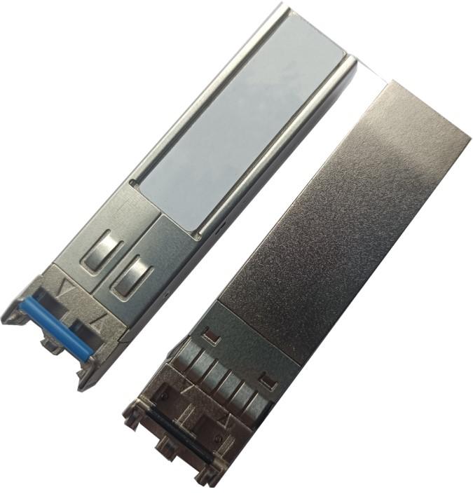
F-tone’s FTCS-xx12-xxDxx series of 1.25G SFP transceiver modules support data rates up to 1.5Gbps, making them the perfect solution for high-speed communication networks. The module is fully compliant with Small Form-Factor Pluggable (SFP) Transceiver Multi-Source Agreement (MSA).
These transceiver modules provide the system designer with reliable solutions for Telecom, Datacom, and other Fibre Channel applications.
Product Features
- VCSEL/FP/DFB Laser Diode Transmitter
- Up to 2 Km on 62.5/125μm MMF, Up to 120 Km on 9/125μm SMF
- 3.3V power supply
- LC duplex optical interface
- LVPECL/CML Differential Input / Output and LVTTL signal detect
- Class 1 Laser International Safety Standard IEC 825 Compliant
- Operating case temperature range: Standard (0 to +70°C) or Industrial (-40°C to +85°C)
- Digital Diagnostic Monitoring (DDM) per SFF-8472
- 2-Wire serial interface (I²C)
- Supports data rates from 100Mbps to 1500Mbps
Applications
- Fiber Channel Switch Infrastructure
- Gigabit Ethernet Switches and Routers
- Other optical links
Absolute Maximum Ratings
Operation beyond the absolute maximum conditions listed in Table 1 will degrade or damage the product. The product is not implied to function above the recommended operating environment; exceeding it may reduce reliability and lifetime.
Table 1 — Absolute Maximum Conditions
| Parameter | Symbol | Min | Max | Units | Note |
|---|---|---|---|---|---|
| Storage Temperature | TST | -40 | +85 | ℃ | – |
| Relative Humidity | RH | 5 | 95 | % | – |
| Supply Voltage | VCC | 0 | +3.6 | V | – |
Table 2 — Recommended Operating Environment and Electrical Characteristics
| Parameter | Symbol | Min | Typ | Max | Units | Note |
|---|---|---|---|---|---|---|
| Supply Voltage | VCC | +3.1 | +3.3 | +3.5 | V | – |
| Supply Current | ICC | – | – | 260 | mA | – |
| Operating Case Temperature (Standard) | TOP | 0 | – | +70 | ℃ | 1 |
| Operating Case Temperature (Industrial) | TOP | -40 | – | +85 | ℃ | 2 |
| Data Rate | B | 100 | 1250 | 1500 | Mbps | – |
Note 1: Standard level Note 2: Industrial level
Optical Parameters
Table 3 — FTCS-8512-02Dxx Optical Characteristics (Ta=+25±5°C, VCC=3.3±0.2V)
| Parameter | Symbol | Min | Typ | Max | Units | Note | |
|---|---|---|---|---|---|---|---|
| Transmitter | |||||||
| Data rate | B | 100 | 1250 | 1500 | Mbps | – | |
| Output Center Wavelength | λc | 830 | 850 | 860 | nm | – | |
| Output Spectral width (RMS) | Δλ | – | – | 0.85 | nm | – | |
| Average Optical Output Power | Po | -12 | – | -3 | dBm | 1,2 | |
| Extinction Ratio | ER | 8.2 | – | – | dB | 1,2 | |
| Optic Output Eye: Compliant IEEE802.3 | 1,2 | ||||||
| Receiver | |||||||
| Receiver Sensitivity | Pmin | – | – | -18 | dBm | 1,2 | |
| Receiver Saturation | Pmax | -3 | – | – | dBm | 1,2 | |
| Operation Center Wavelength | λc | 770 | – | 860 | nm | – | |
| Loss of Signal (Assert) | LOSA | -35 | – | – | dBm | 1,2 | |
| Loss of Signal (Deassert) | LOSD | – | – | -18 | dBm | 1,2 | |
| LOS Hysteresis | LOHYS | 0.5 | – | – | dB | – |
Note 1: The optical power is launched into 62.5/125μm MMF.
Note 2: With a PRBS 2²³⁻¹ test pattern @ 1250Mbps.
Table 4 — FTCS-M1312-02Dxx Optical Characteristics (Ta=+25±5°C, VCC=3.3±0.2V)
| Parameter | Symbol | Min | Typ | Max | Units | Note | |
|---|---|---|---|---|---|---|---|
| Transmitter | |||||||
| Data rate | B | 100 | 1250 | 1500 | Mbps | – | |
| Output Center Wavelength | λc | 1260 | 1310 | 1360 | nm | – | |
| Output Spectral width (RMS) | Δλ | – | – | 4 | nm | – | |
| Average Optical Output Power | Po | -14 | – | -5 | dBm | 1,2 | |
| Extinction Ratio | ER | 8.2 | – | – | dB | 1,2 | |
| Optic Output Eye: Compliant IEEE802.3 | 1,2 | ||||||
| Receiver | |||||||
| Receiver Sensitivity | Pmin | – | – | -23 | dBm | 1,2 | |
| Receiver Saturation | Pmax | -3 | – | – | dBm | 1,2 | |
| Operation Center Wavelength | λc | 1260 | – | 1620 | nm | – | |
| Loss of Signal (Assert) | LOSA | -35 | – | – | dBm | 1,2 | |
| Loss of Signal (Deassert) | LOSD | – | – | -23 | dBm | 1,2 | |
| LOS Hysteresis | LOHYS | 0.5 | – | – | dB | – |
Note 1: The optical power is launched into 62.5/125μm MMF.
Note 2: With a PRBS 2²³⁻¹ test pattern @ 1250Mbps.
Table 5 — FTCS-1312-10Dxx / FTCS-1312-20Dxx Optical Characteristics (Ta=+25±5°C, VCC=3.3±0.2V)
| Parameter | Symbol | Min | Typ | Max | Units | Note | |
|---|---|---|---|---|---|---|---|
| Transmitter | |||||||
| Data rate | B | 100 | 1250 | 1500 | Mbps | – | |
| Output Center Wavelength | λc | 1260 | 1310 | 1360 | nm | – | |
| Output Spectral width (RMS) | Δλ | – | – | 4 | nm | – | |
| Average Optical Output Power | Po | -10 | – | -3 | dBm | 1,2 | |
| Extinction Ratio | ER | 8.2 | – | – | dB | 1,2 | |
| Optic Output Eye: Compliant IEEE802.3 | 1,2 | ||||||
| Receiver | |||||||
| Receiver Sensitivity | Pmin | – | – | -23 | dBm | 1,2 | |
| Receiver Saturation | Pmax | -3 | – | – | dBm | 1,2 | |
| Operation Center Wavelength | λc | 1260 | – | 1620 | nm | – | |
| Loss of Signal (Assert) | LOSA | -35 | – | – | dBm | 1,2 | |
| Loss of Signal (Deassert) | LOSD | – | – | -23 | dBm | 1,2 | |
| LOS Hysteresis | LOHYS | 0.5 | – | – | dB | – |
Note 1: The optical power is launched into 9/125μm SMF.
Note 2: With a PRBS 2²³⁻¹ test pattern @ 1250Mbps.
Table 6 — FTCS-1312-40Dxx Optical Characteristics (Ta=+25±5°C, VCC=3.3±0.2V)
| Parameter | Symbol | Min | Typ | Max | Units | Note | |
|---|---|---|---|---|---|---|---|
| Transmitter | |||||||
| Data rate | B | 100 | 1250 | 1500 | Mbps | – | |
| Output Center Wavelength | λc | 1260 | 1310 | 1360 | nm | – | |
| Output Spectral width (-20dB) | Δλ | – | – | 1 | nm | – | |
| Average Optical Output Power | Po | -5 | – | 0 | dBm | 1,2 | |
| Extinction Ratio | ER | 8.2 | – | – | dB | 1,2 | |
| Optic Output Eye: Compliant IEEE802.3 | 1,2 | ||||||
| Receiver | |||||||
| Receiver Sensitivity | Pmin | – | – | -24 | dBm | 1,2 | |
| Receiver Saturation | Pmax | -3 | – | – | dBm | 1,2 | |
| Operation Center Wavelength | λc | 1260 | – | 1620 | nm | – | |
| Loss of Signal (Assert) | LOSA | -35 | – | – | dBm | 1,2 | |
| Loss of Signal (Deassert) | LOSD | – | – | -24 | dBm | 1,2 | |
| LOS Hysteresis | LOHYS | 0.5 | – | – | dB | – |
Note 1: The optical power is launched into 9/125μm SMF.
Note 2: With a PRBS 2²³⁻¹ test pattern @ 1250Mbps.
Table 7 — FTCS-1512-20Dxx Optical Characteristics (Ta=+25±5°C, VCC=3.3±0.2V)
| Parameter | Symbol | Min | Typ | Max | Units | Note | |
|---|---|---|---|---|---|---|---|
| Transmitter | |||||||
| Data rate | B | 100 | 1250 | 1500 | Mbps | – | |
| Output Center Wavelength | λc | 1480 | 1550 | 1580 | nm | – | |
| Output Spectral width (-20dB) | Δλ | – | – | 1 | nm | – | |
| Average Optical Output Power | Po | -10 | – | -3 | dBm | 1,2 | |
| Extinction Ratio | ER | 8.2 | – | – | dB | 1,2 | |
| Optic Output Eye: Compliant IEEE802.3 | 1,2 | ||||||
| Receiver | |||||||
| Receiver Sensitivity | Pmin | – | – | -23 | dBm | 1,2 | |
| Receiver Saturation | Pmax | -3 | – | – | dBm | 1,2 | |
| Operation Center Wavelength | λc | 1260 | – | 1620 | nm | – | |
| Loss of Signal (Assert) | LOSA | -35 | – | – | dBm | 1,2 | |
| Loss of Signal (Deassert) | LOSD | – | – | -23 | dBm | 1,2 | |
| LOS Hysteresis | LOHYS | 0.5 | – | – | dB | – |
Note 1: The optical power is launched into 9/125μm SMF.
Note 2: With a PRBS 2²³⁻¹ test pattern @ 1250Mbps.
Table 8 — FTCS-1512-40Dxx Optical Characteristics (Ta=+25±5°C, VCC=3.3±0.2V)
| Parameter | Symbol | Min | Typ | Max | Units | Note | |
|---|---|---|---|---|---|---|---|
| Transmitter | |||||||
| Data rate | B | 100 | 1250 | 1500 | Mbps | – | |
| Output Center Wavelength | λc | 1480 | 1550 | 1580 | nm | – | |
| Output Spectral width (-20dB) | Δλ | – | – | 1 | nm | – | |
| Average Optical Output Power | Po | -8 | – | -3 | dBm | 1,2 | |
| Extinction Ratio | ER | 8.2 | – | – | dB | 1,2 | |
| Optic Output Eye: Compliant IEEE802.3 | 1,2 | ||||||
| Receiver | |||||||
| Receiver Sensitivity | Pmin | – | – | -25 | dBm | 1,2 | |
| Receiver Saturation | Pmax | -3 | – | – | dBm | 1,2 | |
| Operation Center Wavelength | λc | 1260 | – | 1620 | nm | – | |
| Loss of Signal (Assert) | LOSA | -35 | – | – | dBm | 1,2 | |
| Loss of Signal (Deassert) | LOSD | – | – | -25 | dBm | 1,2 | |
| LOS Hysteresis | LOHYS | 0.5 | – | – | dB | – |
Note 1: The optical power is launched into 9/125μm SMF.
Note 2: With a PRBS 2²³⁻¹ test pattern @ 1250Mbps.
Table 9 — FTCS-1512-60Dxx Optical Characteristics (Ta=+25±5°C, VCC=3.3±0.2V)
| Parameter | Symbol | Min | Typ | Max | Units | Note | |
|---|---|---|---|---|---|---|---|
| Transmitter | |||||||
| Data rate | B | 100 | 1250 | 1500 | Mbps | – | |
| Output Center Wavelength | λc | 1480 | 1550 | 1580 | nm | – | |
| Output Spectral width (-20dB) | Δλ | – | – | 1 | nm | – | |
| Average Optical Output Power | Po | -5 | – | 0 | dBm | 1,2 | |
| Extinction Ratio | ER | 8.2 | – | – | dB | 1,2 | |
| Optic Output Eye: Compliant IEEE802.3 | 1,2 | ||||||
| Receiver | |||||||
| Receiver Sensitivity | Pmin | – | – | -25 | dBm | 1,2 | |
| Receiver Saturation | Pmax | -3 | – | – | dBm | 1,2 | |
| Operation Center Wavelength | λc | 1260 | – | 1620 | nm | – | |
| Loss of Signal (Assert) | LOSA | -35 | – | – | dBm | 1,2 | |
| Loss of Signal (Deassert) | LOSD | – | – | -25 | dBm | 1,2 | |
| LOS Hysteresis | LOHYS | 0.5 | – | – | dB | – |
Note 1: The optical power is launched into 9/125μm SMF.
Note 2: With a PRBS 2²³⁻¹ test pattern @ 1250Mbps.
Table 10 — FTCS-1512-80Dxx Optical Characteristics (Ta=+25±5°C, VCC=3.3±0.2V)
| Parameter | Symbol | Min | Typ | Max | Units | Note | |
|---|---|---|---|---|---|---|---|
| Transmitter | |||||||
| Data rate | B | 100 | 1250 | 1500 | Mbps | – | |
| Output Center Wavelength | λc | 1480 | 1550 | 1580 | nm | – | |
| Output Spectral width (-20dB) | Δλ | – | – | 1 | nm | – | |
| Average Optical Output Power | Po | -2 | – | +3 | dBm | 1,2 | |
| Extinction Ratio | ER | 8.2 | – | – | dB | 1,2 | |
| Optic Output Eye: Compliant IEEE802.3 | 1,2 | ||||||
| Receiver | |||||||
| Receiver Sensitivity | Pmin | – | – | -26 | dBm | 1,2 | |
| Receiver Saturation | Pmax | -3 | – | – | dBm | 1,2 | |
| Operation Center Wavelength | λc | 1260 | – | 1620 | nm | – | |
| Loss of Signal (Assert) | LOSA | -35 | – | – | dBm | 1,2 | |
| Loss of Signal (Deassert) | LOSD | – | – | -26 | dBm | 1,2 | |
| LOS Hysteresis | LOHYS | 0.5 | – | – | dB | – |
Note 1: The optical power is launched into 9/125μm SMF.
Note 2: With a PRBS 2²³⁻¹ test pattern @ 1250Mbps.
Table 11 — FTCS-1512-H0Dxx Optical Characteristics (Ta=+25±5°C, VCC=3.3±0.2V)
| Parameter | Symbol | Min | Typ | Max | Units | Note | |
|---|---|---|---|---|---|---|---|
| Transmitter | |||||||
| Data rate | B | 100 | 1250 | 1500 | Mbps | – | |
| Output Center Wavelength | λc | 1480 | 1550 | 1580 | nm | – | |
| Output Spectral width (-20dB) | Δλ | – | – | 1 | nm | – | |
| Average Optical Output Power | Po | 0 | – | +5 | dBm | 1,2 | |
| Extinction Ratio | ER | 8.2 | – | – | dB | 1,2 | |
| Optic Output Eye: Compliant IEEE802.3 | 1,2 | ||||||
| Receiver | |||||||
| Receiver Sensitivity | Pmin | – | – | -28 | dBm | 1,2 | |
| Receiver Saturation | Pmax | -3 | – | – | dBm | 1,2 | |
| Operation Center Wavelength | λc | 1260 | – | 1620 | nm | – | |
| Loss of Signal (Assert) | LOSA | -35 | – | – | dBm | 1,2 | |
| Loss of Signal (Deassert) | LOSD | – | – | -28 | dBm | 1,2 | |
| LOS Hysteresis | LOHYS | 0.5 | – | – | dB | – |
Note 1: The optical power is launched into 9/125μm SMF.
Note 2: With a PRBS 2²³⁻¹ test pattern @ 1250Mbps.
Table 12 — FTCS-1512-H2Dxx Optical Characteristics (Ta=+25±5°C, VCC=3.3±0.2V)
| Parameter | Symbol | Min | Typ | Max | Units | Note | |
|---|---|---|---|---|---|---|---|
| Transmitter | |||||||
| Data rate | B | 100 | 1250 | 1500 | Mbps | – | |
| Output Center Wavelength | λc | 1480 | 1550 | 1580 | nm | – | |
| Output Spectral width (-20dB) | Δλ | – | – | 1 | nm | – | |
| Average Optical Output Power | Po | 0 | – | +5 | dBm | 1,2 | |
| Extinction Ratio | ER | 8.2 | – | – | dB | 1,2 | |
| Optic Output Eye: Compliant IEEE802.3 | 1,2 | ||||||
| Receiver | |||||||
| Receiver Sensitivity | Pmin | – | – | -30 | dBm | 1,2 | |
| Receiver Saturation | Pmax | -3 | – | – | dBm | 1,2 | |
| Operation Center Wavelength | λc | 1260 | – | 1620 | nm | – | |
| Loss of Signal (Assert) | LOSA | -40 | – | – | dBm | 1,2 | |
| Loss of Signal (Deassert) | LOSD | – | – | -30 | dBm | 1,2 | |
| LOS Hysteresis | LOHYS | 0.5 | – | – | dB | – |
Note 1: The optical power is launched into 9/125μm SMF.
Note 2: With a PRBS 2²³⁻¹ test pattern @ 1250Mbps.
Electrical Parameters
Table 13 — Transceiver Electrical Characteristics (Ta=+25±5°C, VCC=3.3±0.2V)
| Parameter | Symbol | Min | Typ | Max | Units | Note | ||
|---|---|---|---|---|---|---|---|---|
| Supply Voltage | VCC | +3.1 | +3.3 | +3.5 | V | – | ||
| Supply Current | ICC | – | – | 260 | mA | – | ||
| Transmitter | ||||||||
| Differential Input Voltage | Vin | 400 | – | 2000 | mVP-P | – | ||
| Input Differential Impedance | Zin | 90 | 100 | 110 | Ω | – | ||
| TX_DISABLE (Disable) | VD | 2.0 | – | VCC | V | – | ||
| TX_DISABLE (Enable) | VEN | 0 | – | 0.8 | V | – | ||
| TX_Fault (Fault) | VF | 2.0 | – | VCC | V | – | ||
| TX_Fault (Normal) | VN | 0 | – | 0.8 | V | – | ||
| Receiver | ||||||||
| Differential Output Voltage | VOUT | 400 | – | 2000 | mVP-P | – | ||
| RX_LOS (Fault) | VF | 2.0 | – | VCC | V | – | ||
| RX_LOS (Normal) | VN | 0 | – | 0.8 | V | – |
Digital Diagnostic Monitoring Characteristics
Table 14 — Digital Diagnostic Monitoring Characteristics
| Parameter | Symbol | Range | Accuracy | Note |
|---|---|---|---|---|
| Transceiver Internal Temperature | T | Recommended Operation Condition | ±3°C | – |
| Transceiver Internal Supply Voltage | VCC | Recommended Operation Condition | ±3% | – |
| Laser Bias Current | ID | ID: 1-100mA, Recommended Operation Condition | ±10% | – |
| TX Output Power | PO | PO: min~max dBm, Recommended Operation Condition | ±3dBm | – |
| RX Input Power | PI | PI: min~max dBm, Recommended Operation Condition | ±3dBm | – |
EEPROM Information Functions
Serial ID provides access to identification information that describes the transceiver’s capabilities, standard interfaces, manufacturer, and other information. SFP transceivers provide a unique enhanced digital diagnostic monitoring interface, which allows real-time access to device operating parameters such as transceiver temperature, laser bias current, transmitted optical power, received optical power, and transceiver supply voltage.
It also defines a sophisticated system of alarm and warning flags, which alerts end users when particular operating parameters are outside of a factory-set normal range.
Defines a 256-byte memory map in E²PROM that is accessible over a 2-wire serial interface at the 8-bit address 1010000X (A0h). The digital diagnostic monitoring interface makes use of the 8-bit address 1010001X (A2h). The interface is identical to, and compatible with both the GBIC Specification and the SFP Multi-Source Agreement.
Table 15 — Serial ID Memory Map: A0h (Base ID Fields)
| Data Address | Size (Byte) | Name of Field | Description |
|---|---|---|---|
| 0 | 1 | Identifier | SFP |
| 1 | 1 | Ext. Identifier | SFP function is defined by serial ID only |
| 2 | 1 | Connector | LC Connector |
| 3-10 | 8 | Transceiver | Transceiver Codes |
| 11 | 1 | Encoding | NRZ |
| 12 | 1 | BR, Nominal | 1250Mbps |
| 13 | 1 | Reserved | |
| 14 | 1 | Length(9μm)km | Transceiver transmit distance |
| 15 | 1 | Length(9μm)100m | |
| 16 | 1 | Length(50μm)10m | |
| 17 | 1 | Length(62.5μm)10m | |
| 18 | 1 | Length(Copper) | Not compliant |
| 19 | 1 | Reserved | |
| 20-35 | 16 | Vendor Name | SFP vendor name: F-tone |
| 36 | 1 | Reserved | |
| 37-39 | 3 | Vendor OUI | |
| 40-55 | 16 | Vendor PN | Part Number: “FTCS-xx12-xxDxx” |
| 56-59 | 4 | Vendor rev | |
| 60-61 | 2 | Wavelength | Transceiver wavelength |
| 62 | 1 | Reserved | |
| 63 | 1 | CC_BASE | Check code for Base ID Fields |
Table 15 — Serial ID Memory Map: A0h (Extended & Vendor Specific Fields)
| Data Address | Size (Byte) | Name of Field | Description |
|---|---|---|---|
| 64-65 | 2 | Options | TX_FAULT, TX_DISABLE and Loss of Signal implemented |
| 66 | 1 | BR, max | |
| 67 | 1 | BR, min | |
| 68-83 | 16 | Vendor SN | Serial number |
| 84-91 | 8 | Date code | Manufacture date code |
| 92 | 1 | Diagnostic Monitoring Type | Digital diagnostic monitoring implemented, “internally calibrated”, RX measurement type is “Average Power” |
| 93 | 1 | Enhanced Options | Optional Alarm/Warning flags for all monitored quantities, Optional Soft RX_LOS monitoring |
| 94 | 1 | SFF-8472 Compliance | Includes functionality described in Rev 9.3 SFF-8472 |
| 95 | 1 | CC_EXT | Check sum for the extended ID Fields |
| 96-127 | 32 | Vendor Specific | Vendor Specific EEPROM |
| 128-255 | 128 | Reserved | Reserved for SFF-8079 |
Pin Definitions
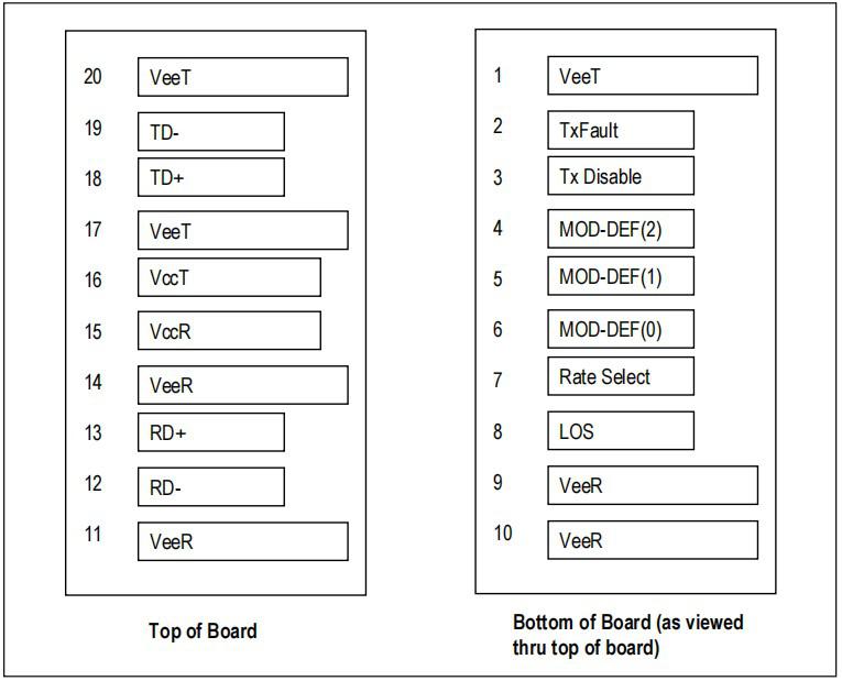
Table 16 — Connector Pin Assignment
| Pin # | Pin Name | Plug Seq. | Description | Note |
|---|---|---|---|---|
| 1 | VeeT | 1 | Transmitter Ground | 6 |
| 2 | TX Fault | 3 | Transmitter Fault Indication | 1 |
| 3 | TX Disable | 3 | Transmitter Disable | 2 |
| 4 | MOD_DEF(2) | 3 | SDA Serial Data Signal | 3 |
| 5 | MOD_DEF(1) | 3 | SCL Serial Clock Signal | 3 |
| 6 | MOD_DEF(0) | 3 | Grounded to indicate module presence | 3 |
| 7 | Rate Select | 3 | Not in used | 4 |
| 8 | LOS | 3 | Loss of Signal | 5 |
| 9 | VeeR | 1 | Receiver Ground | 6 |
| 10 | VeeR | 1 | Receiver Ground | 6 |
| 11 | VeeR | 1 | Receiver Ground | 6 |
| 12 | RD- | 3 | Inv. Received Data Out | 8 |
| 13 | RD+ | 3 | Received Data Out | 8 |
| 14 | VeeR | 1 | Receiver Ground | 6 |
| 15 | VccR | 2 | Receiver Power | 7 |
| 16 | VccT | 2 | Transmitter Power | 7 |
| 17 | VeeT | 1 | Transmitter Ground | 6 |
| 18 | TD+ | 3 | Transmit Data In | 9 |
| 19 | TD- | 3 | Inv. Transmit Data In | 9 |
| 20 | VeeT | 1 | Transmitter Ground | 6 |
Plug Seq.: Pin engagement sequence during hot plugging.
Pin Function Notes
Note 1 — TX_Fault: Open collector/drain output, should be pulled up with a 4.7kΩ–10kΩ resistor on the host board. Pull-up voltage between 2.0V and VCCT+0.3V. When high, output indicates a laser fault. Low indicates normal operation (< 0.8V).
Note 2 — TX_Disable: Input for shutting down the transmitter optical output.
Low (0–0.8V): Transmitter on | (>0.8, <2.0V): Undefined | High (2.0–VCC): Transmitter Disabled | Open: Transmitter Disabled
Note 3 — Mod-Def 0, 1, 2: Module definition pins, should be pulled up with a 4.7kΩ–10kΩ resistor. Mod-Def 0 is grounded by the module to indicate presence. Mod-Def 1 is the clock line of the 2-wire serial interface. Mod-Def 2 is the data line.
Note 4: Not in used.
Note 5 — LOS: Open collector/drain output, pulled up with a 4.7kΩ–10kΩ resistor. When high, indicates received optical power is below worst-case receiver sensitivity. Low indicates normal operation (< 0.8V).
Note 6: VeeR and VeeT may be internally connected within the SFP module.
Note 7: VccR and VccT are the receiver and transmitter power supplies, defined as 3.3V ±5%. Maximum supply current is 300mA. VccR and VccT may be internally connected.
Note 8: RD-/+: Differential receiver outputs, AC-coupled 100Ω differential lines. AC coupling is done inside the module.
Note 9: TD-/+: Differential transmitter inputs, AC-coupled with 100Ω differential terminations inside the module.
Host Board Layout
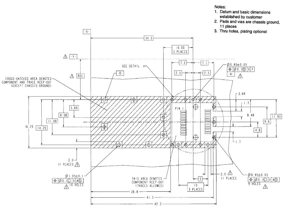
A typical host board mechanical layout for attaching the SFP Connector and Cage System.
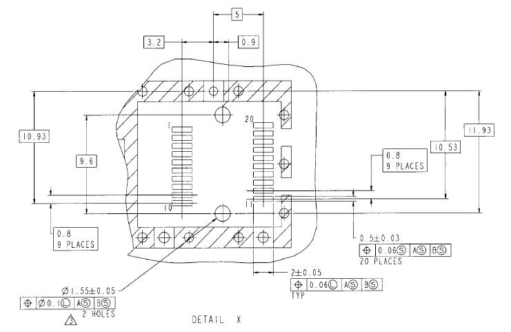
SFP Host Board Mechanical Layout (Cont.)
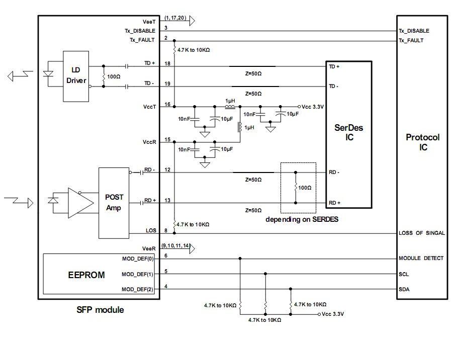
Recommended Circuit Schematic
Module Outline Drawing
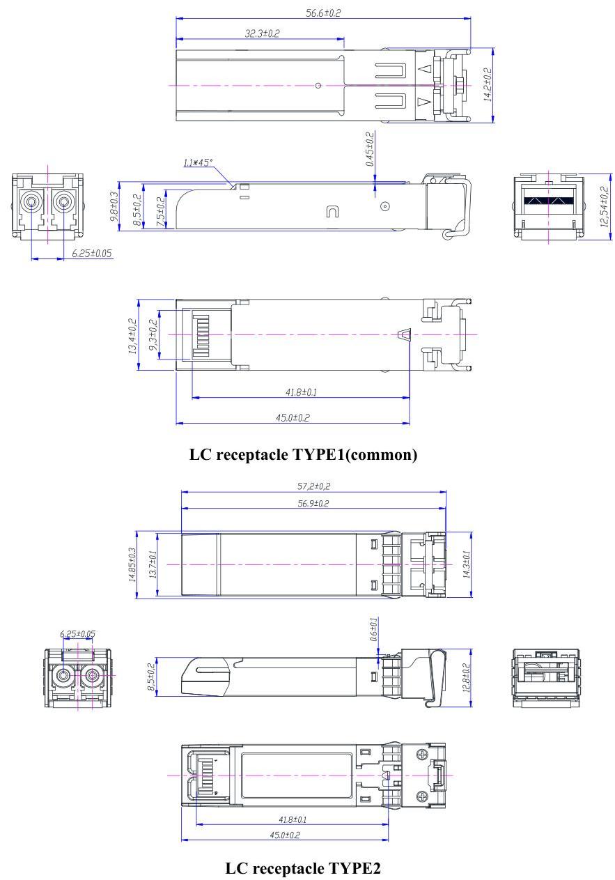
Units in mm. Specifications subject to change without notice.
Ordering Information
| Part Number | Product Description |
|---|---|
| FTCS-8512-02D | SFP Transceiver Module, MMF, 850nm, 1.25G, 0.5km, with DDM, 0°C~+70°C |
| FTCS-8512-02DI | SFP Transceiver Module, MMF, 850nm, 1.25G, 0.5km, with DDM, -40°C~+85°C |
| FTCS-M1312-02D | SFP Transceiver Module, MMF, 1310nm, 1.25G, 0.55km, with DDM, 0°C~+70°C |
| FTCS-M1312-02DI | SFP Transceiver Module, MMF, 1310nm, 1.25G, 0.55km, with DDM, -40°C~+85°C |
| FTCS-1312-10D | SFP Transceiver Module, 1310nm, 1.25G, 10km, with DDM, 0°C~+70°C |
| FTCS-1312-10DI | SFP Transceiver Module, 1310nm, 1.25G, 10km, with DDM, -40°C~+85°C |
| FTCS-1312-20D | SFP Transceiver Module, 1310nm, 1.25G, 20km, with DDM, 0°C~+70°C |
| FTCS-1312-20DI | SFP Transceiver Module, 1310nm, 1.25G, 20km, with DDM, -40°C~+85°C |
| FTCS-1312-40D | SFP Transceiver Module, 1310nm, 1.25G, 40km, with DDM, 0°C~+70°C |
| FTCS-1312-40DI | SFP Transceiver Module, 1310nm, 1.25G, 40km, with DDM, -40°C~+85°C |
| FTCS-1512-20D | SFP Transceiver Module, 1550nm, 1.25G, 20km, with DDM, 0°C~+70°C |
| FTCS-1512-20DI | SFP Transceiver Module, 1550nm, 1.25G, 20km, with DDM, -40°C~+85°C |
| FTCS-1512-40D | SFP Transceiver Module, 1550nm, 1.25G, 40km, with DDM, 0°C~+70°C |
| FTCS-1512-40DI | SFP Transceiver Module, 1550nm, 1.25G, 40km, with DDM, -40°C~+85°C |
| FTCS-1512-60D | SFP Transceiver Module, 1550nm, 1.25G, 60km, with DDM, 0°C~+70°C |
| FTCS-1512-60DI | SFP Transceiver Module, 1550nm, 1.25G, 60km, with DDM, -40°C~+85°C |
| FTCS-1512-80D | SFP Transceiver Module, 1550nm, 1.25G, 80km, with DDM, 0°C~+70°C |
| FTCS-1512-80DI | SFP Transceiver Module, 1550nm, 1.25G, 80km, with DDM, -40°C~+85°C |
| FTCS-1512-H0D | SFP Transceiver Module, 1550nm, 1.25G, 100km, with DDM, 0°C~+70°C |
| FTCS-1512-H0DI | SFP Transceiver Module, 1550nm, 1.25G, 100km, with DDM, -40°C~+85°C |
| FTCS-1512-H2D | SFP Transceiver Module, 1550nm, 1.25G, 120km, with DDM, 0°C~+70°C |
| FTCS-1512-H2DI | SFP Transceiver Module, 1550nm, 1.25G, 120km, with DDM, -40°C~+85°C |
Contact Information
| Item | Details |
|---|---|
| Company | 北亿纤通 | F-tone Networks |
| Region | 中国四川天府新区 |
| Service Area | 全球 (Global) |
| Phone | 028-85255257 |
| Fax | 028-85977702 |
| Mobile | 19081343401 |
| Website | https://www.f-tone.com |
| HR | hr@f-tone.com |
| Sales | sales@f-tone.com |
| Technical Support | support@f-tone.com |
本产品为 1.25G SFP Transceiver Module (FTCS-xx12-xxDxx系列) 产品线,详细信息,请联系我们的销售人员,谢谢!
Important Notice
Performance figures, data and any illustrative material provided in this data sheet are typical and must be specifically confirmed in writing by F-tone Networks before they become applicable to any particular order or contract. In accordance with the F-tone Networks policy of continuous improvement specifications may change without notice.
The publication of information in this data sheet does not imply freedom from patent or other protective rights of F-tone Networks or others. Further details are available from any F-tone Networks sales representative.