
Product Overview
The FTCS-131X-02Dxx is a high-performance 10.3Gbps SFP+ optical transceiver designed for single-mode fiber transmission up to 2km. It features an un-cooled 1310nm FP laser transmitter and PIN photo detector receiver, providing cost-effective and reliable 10G connectivity for optical systems and LTE applications.
The module is hot-pluggable with a duplex LC receptacle interface, compliant with SFP+ MSA and SFF-8472 standards. It supports real-time digital diagnostic monitoring and operates on a single +3.3V power supply with power dissipation below 1.2W.

Key Features
- Supports 10.3Gbps bit rates
- Hot-pluggable SFP+ footprint
- Un-cooled 1310nm FP laser transmitter
- PIN photo detector receiver with integrated TIA
- Up to 2km transmission over single-mode fiber (SMF)
- Compliant with SFP+ MSA and SFF-8472
- Duplex LC receptacle connector
- Compatible with RoHS
- Single +3.3V power supply
- Power dissipation <1.2W
- Real-time Digital Diagnostic Monitoring (DDM)
- SFI electrical interface
- Operating case temperature: 0 to +70°C (Standard), -40 to +85°C (Industrial)
Applications
- 10Gbps Optical Systems
- LTE Systems
- Other Optical Links
- Telecommunications Networks
- Data Center Interconnects
Product Description
The SFP+ transceivers are high-performance, cost-effective modules supporting data rate of 10Gbps and 2km transmission distance with SMF. The transceiver consists of three sections: a FP laser transmitter, a PIN photodiode integrated with a trans-impedance preamplifier (TIA), and MCU control unit. All modules satisfy class I laser safety requirements.
The transceivers are compatible with SFP Multi-Source Agreement and SFF-8472 digital diagnostics functions.
Absolute Maximum Ratings
| Parameter | Symbol | Min | Max | Unit |
|---|---|---|---|---|
| Supply Voltage | Vcc | -0.5 | 4.5 | V |
| Storage Temperature | Ts | -40 | +85 | °C |
| Operating Humidity | – | 5 | 85 | % |
Recommended Operating Conditions
| Parameter | Symbol | Min | Typical | Max | Unit |
|---|---|---|---|---|---|
| Operating Case Temperature (Standard) | Tc | 0 | – | +70 | °C |
| Operating Case Temperature (Extended) | Tc | -20 | – | +80 | °C |
| Operating Case Temperature (Industrial) | Tc | -40 | – | +85 | °C |
| Power Supply Voltage | Vcc | 3.135 | 3.30 | 3.465 | V |
| Power Supply Current | Icc | – | 350 | – | mA |
| Data Rate | – | 1.0 | 10.3 | 10.7 | Gbps |
Optical and Electrical Characteristics – Transmitter
| Parameter | Symbol | Min | Typical | Max | Unit | Notes |
|---|---|---|---|---|---|---|
| Centre Wavelength | λc | 1270 | 1310 | 1350 | nm | |
| Spectral Width (RMS) | Δλ | – | – | 3 | nm | |
| Side-Mode Suppression Ratio | SMSR | – | – | – | dB | |
| Average Output Power | Pout | -6.5 | – | -0.5 | dBm | 1 |
| Extinction Ratio | ER | 4.0 | – | – | dB | |
| Output Eye Diagram Margin | – | 15 | – | – | % | 5 |
| Data Input Swing Differential | VIN | 180 | – | 850 | mV | 2 |
| Input Differential Impedance | ZIN | 90 | 100 | 110 | Ω | |
| TX Disable – Disable | – | 2.0 | – | Vcc | V | |
| TX Disable – Enable | – | 0 | – | 0.8 | V | |
| TX Fault – Fault | – | 2.0 | – | Vcc | V | |
| TX Fault – Normal | – | 0 | – | 0.8 | V |
Optical and Electrical Characteristics – Receiver
| Parameter | Symbol | Min | Typical | Max | Unit | Notes |
|---|---|---|---|---|---|---|
| Centre Wavelength | λc | 1260 | – | 1600 | nm | |
| Receiver Sensitivity | – | – | – | -14.4 | dBm | 3 |
| Receiver Overload | – | – | 0.5 | – | dBm | 3 |
| LOS De-Assert | LOSD | – | – | -15.5 | dBm | |
| LOS Assert | LOSA | -30 | – | – | dBm | |
| LOS Hysteresis | – | 0.5 | – | – | dB | |
| Data Output Swing Differential | Vout | 300 | – | 900 | mV | 4 |
| LOS – High | – | 2.0 | – | Vcc | V | |
| LOS – Low | – | – | – | 0.8 | V |
Notes: 1) The optical power is launched into SMF. 2) PECL input, internally AC-coupled and terminated. 3) Measured with a PRBS 2³¹-1 test pattern @10312Mbps, BER ≤1×10⁻¹². 4) Internally AC-coupled. 5) Compliant with ITUT and IEEE recommendation MASK.
Timing Characteristics
| Parameter | Symbol | Min | Typical | Max | Unit |
|---|---|---|---|---|---|
| Tx Disable Negate Time | t_on | – | – | 1 | ms |
| Tx Disable Assert Time | t_off | – | – | 10 | µs |
| Time To Initialize (including Reset of Tx Fault) | t_init | – | – | 300 | ms |
| Tx Fault Assert Time | t_fault | – | – | 100 | µs |
| Tx Disable To Reset | t_reset | 10 | – | – | µs |
| LOS Assert Time | t_loss_on | – | – | 100 | µs |
| LOS De-assert Time | t_loss_off | – | – | 100 | µs |
| Serial ID Clock Rate | f_serial_clock | – | 100 | 400 | KHz |
| MOD_DEF (0:2) – High | VH | 2 | – | Vcc | V |
| MOD_DEF (0:2) – Low | VL | – | – | 0.8 | V |
Diagnostics
| Parameter | Range | Unit | Accuracy | Calibration |
|---|---|---|---|---|
| Temperature | 0 to +70 / -20 to +80 / -40 to +85 | °C | ±3°C | Internal |
| Voltage | 3.0 to 3.6 | V | ±3% | Internal |
| Bias Current | 0 to 100 | mA | ±10% | Internal |
| TX Power | -6.5 to -0.5 | dBm | ±3dB | Internal |
| RX Power | -14.4 to -1 | dBm | ±3dB | Internal |
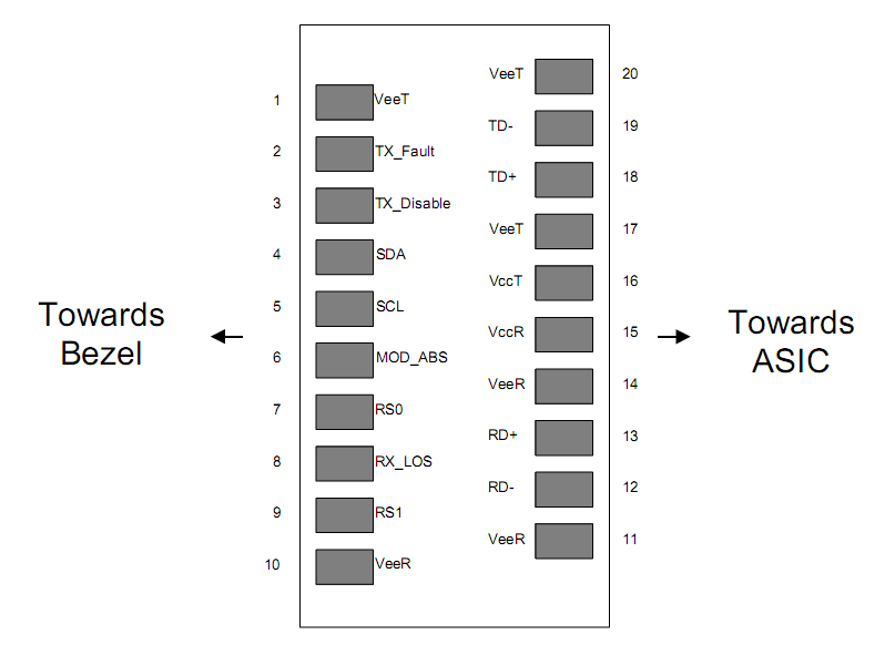
Pin Descriptions
| Pin | Signal Name | Description | Plug Seq. | Notes |
|---|---|---|---|---|
| 1 | VEET | Transmitter Ground | 1 | |
| 2 | TX FAULT | Transmitter Fault Indication | 3 | Note 1 |
| 3 | TX DISABLE | Transmitter Disable | 3 | Note 2 |
| 4 | SDA | SDA Serial Data Signal | 3 | |
| 5 | SCL | SCL Serial Clock Signal | 3 | |
| 6 | MOD_ABS | Module Absent. Grounded within the module | 3 | |
| 7 | RS0 | Not Connected | 3 | |
| 8 | LOS | Loss of Signal | 3 | Note 3 |
| 9 | RS1 | Not Connected | 3 | |
| 10 | VEER | Receiver Ground | 1 | |
| 11 | VEER | Receiver Ground | 1 | |
| 12 | RD- | Inverted Received Data Out | 3 | Note 4 |
| 13 | RD+ | Received Data Out | 3 | Note 4 |
| 14 | VEER | Receiver Ground | 1 | |
| 15 | VCCR | Receiver Power Supply | 2 | |
| 16 | VCCT | Transmitter Power Supply | 2 | |
| 17 | VEET | Transmitter Ground | 1 | |
| 18 | TD+ | Transmit Data In | 3 | Note 5 |
| 19 | TD- | Inverted Transmit Data In | 3 | Note 5 |
| 20 | VEET | Transmitter Ground | 1 |
Notes: Plug Seq. indicates pin engagement sequence during hot plugging.
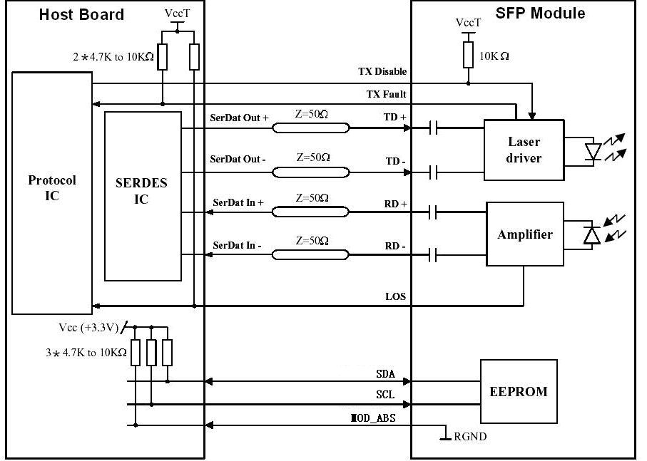
1) TX Fault is an open collector output, which should be pulled up with a 4.7k~10kΩ resistor on the host board to a voltage between 2.0V and Vcc+0.3V. Logic 0 indicates normal operation; Logic 1 indicates a laser fault.
2) Laser output disabled on TDIS >2.0V or open, enabled on TDIS <0.8V.
3) LOS is open collector output. Should be pulled up with 4.7k~10kΩ on host board to a voltage between 2.0V and 3.6V. Logic 0 indicates normal operation; logic 1 indicates loss of signal.
4) RD-/+: These are the differential receiver outputs. They are internally AC-coupled 100Ω differential lines which should be terminated with 100Ω (differential) at the user SERDES.
5) TD-/+: These are the differential transmitter inputs. They are internally AC-coupled, differential lines with 100Ω differential termination inside the module.
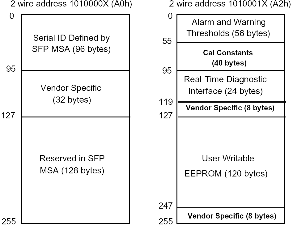
Digital Diagnostic Memory Map
The transceivers provide serial ID memory contents and diagnostic information about the present operating conditions by the 2-wire serial interface (SCL, SDA). The diagnostic information with internal calibration or external calibration are all implemented, including received power monitoring, transmitted power monitoring, bias current monitoring, supply voltage monitoring, and temperature monitoring.
Ordering Information
| Part Number | Product Description |
|---|---|
| FTCS-131X-02D | 1310nm, 10Gbps, LC, 2km, 0°C~+70°C, with DDM |
| FTCS-131X-02DI | 1310nm, 10Gbps, LC, 2km, -40°C~+85°C, with DDM |
Region: Tianfu New Area, Sichuan, China
Service Area: Global
Tel: 028-85255257 | Fax: 028-85977702 | Mobile: 19081343401
Site: https://www.f-tone.com
HR: hr@f-tone.com | Sales: sales@f-tone.com | Support: support@f-tone.com
本产品为【10G光模块】产品线,详细信息,请联系我们的销售人员,谢谢!