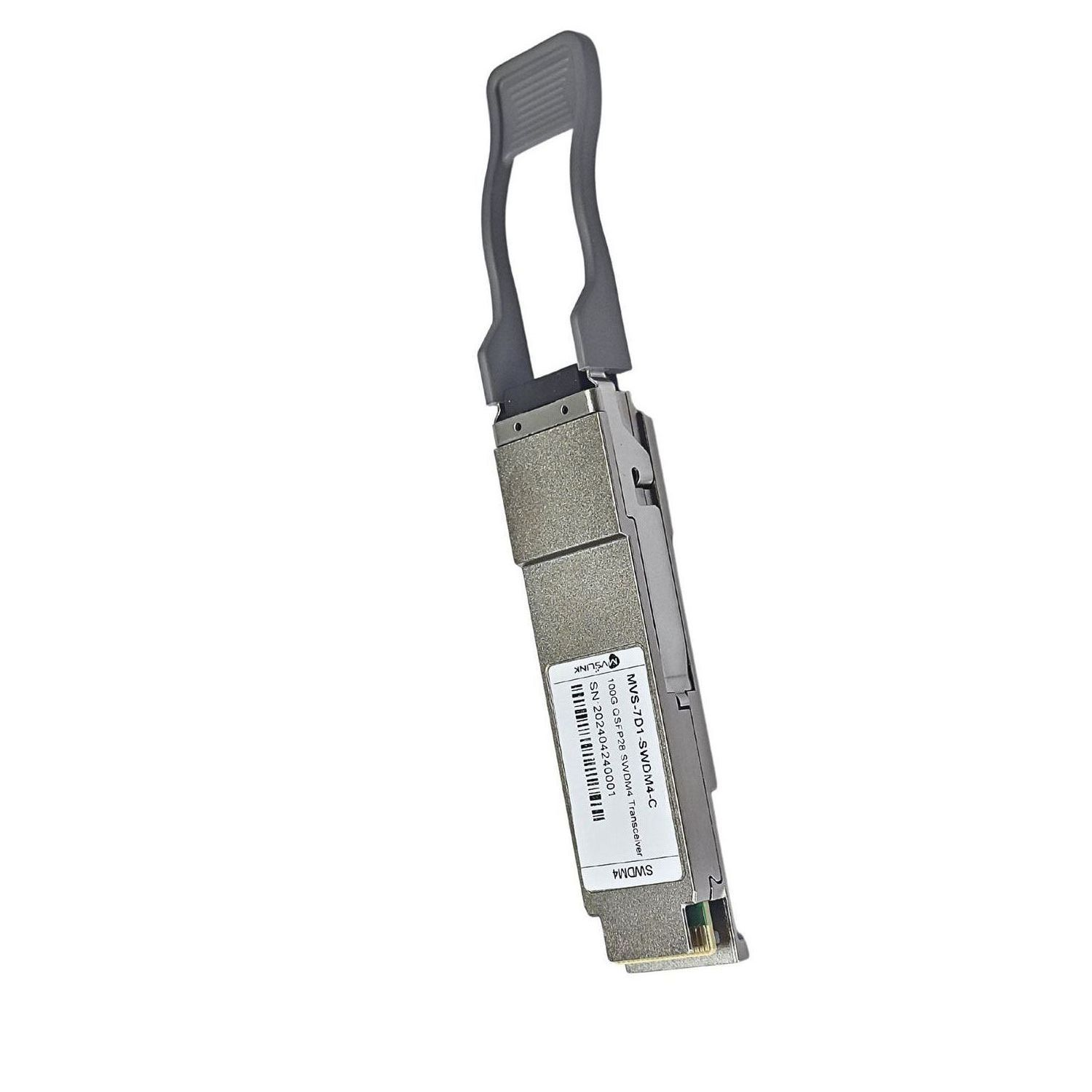
FTQ2-HG-SWDM4 is a QSFP28 100G SWDM4 optical transceiver module designed for use in 100G Ethernet links over duplex multimode fiber. It utilizes four channels/lanes in the 850–940nm region @25.78Gbps to transport the Ethernet signal. Digital diagnostics functions are available via an I²C interface, as specified by the QSFP28 MSA.
Features
- Compliant with QSFP28 MSA
- Compliant with SWDM MSA
- Compliant with IEEE 802.3bm CAUI-4
- Hot-pluggable QSFP28 form factor
- 4×25Gb/s 850nm VCSEL-based transmitter
- Supports 103.1Gbps aggregate bit rate
- Power dissipation < 3.5W
- Maximum link length of 150m on OM5 multimode fiber
- Case temperature range of 0°C to 70°C
- Duplex LC receptacles
- CAUI-4 electrical interface
- RoHS compliant
Applications
- 100G Ethernet over Duplex MMF
Absolute Maximum Ratings
| Parameter | Symbol | Min. | Max. | Units |
|---|---|---|---|---|
| Storage Temp Range | Ts | -40 | +85 | ℃ |
| Supply Voltage | Vcc | -0.5 | 3.6 | V |
| Relative Humidity | RH | 15% | 85% | – |
Operating Conditions
| Characteristic | Symbol | Min. | Max. | Units |
|---|---|---|---|---|
| Case Temp – Operating | Tcase | 0 | 70 | ℃ |
| Supply Voltage | Vcc | 3.14 | 3.46 | V |
Optical Characteristics – Transmitter
| Transmitter Parameter | Lane | Min | Typical | Max | Unit |
|---|---|---|---|---|---|
| Power Consumption | – | – | – | 3.5 | W |
| Signaling rate, each lane | – | – | 25.78125±100ppm | – | Gb/s |
| Link Distance on OM3 Fiber | – | – | – | 75 | m |
| Lane Wavelength Range | Lane 0 | 844 | – | 874 | nm |
| Lane Wavelength Range | Lane 1 | 875 | – | 893 | nm |
| Lane Wavelength Range | Lane 2 | 894 | – | 918 | nm |
| Lane Wavelength Range | Lane 3 | 919 | – | 948 | nm |
| Link Distance on OM4 Fiber | – | – | – | 100 | m |
| Modulation Format | – | – | NRZ | – | – |
| Link Distance on OM5 Fiber | – | – | – | 150 | m |
| Difference in launch power between any two lanes | – | – | – | 4.5 | dB |
| RMS Spectral Width | – | – | – | 0.59 | nm |
| Optical Modulation Amplitude (OMA), each lane | – | -5.5 | – | 3 | dBm |
| Average Launch Power per Lane @TX | – | -5.5 | – | 3 | dBm |
| Off State | – | -30 | – | – | dBm |
| Launch Power in OMA minus TDEC, each lane | – | -7 | – | – | dBm |
| Transmitter and Dispersion Eye Closure (TDEC) | – | – | – | 4 | dB |
| Extinction Ratio | – | 2 | – | – | dB |
| Damage Threshold | – | – | – | 4.4 | dBm |
| Optical Return Loss Tolerance | – | – | – | 12 | dB |
| Transmitter Eye Mask Definition {X1,X2,X3,Y1,Y2,Y3} | – | {0.3,0.38,0.45,0.35,0.41,0.5} | – | – | – |
Optical Characteristics – Receiver
| Receiver Parameter | Lane | Min | Typical | Max | Unit |
|---|---|---|---|---|---|
| Signaling rate, each lane | – | – | 25.78125±100ppm | – | Gb/s |
| Lane Wavelength Range | Lane 0 | 844 | – | 874 | nm |
| Lane Wavelength Range | Lane 1 | 875 | – | 893 | nm |
| Lane Wavelength Range | Lane 2 | 894 | – | 918 | nm |
| Lane Wavelength Range | Lane 3 | 919 | – | 948 | nm |
| Modulation Format | – | – | NRZ | – | – |
| Damage Threshold | – | – | – | 4.4 | dBm |
| Optical Return Loss Tolerance | – | – | – | 12 | dB |
| Average Receive Power, each lane | – | – | – | 3.4 | dBm |
| Encircled Flux | – | ≥86% at 19um / ≤30% at 4.5um | – | – | – |
| Receiver Power, each lane (OMA) | – | -9.5 | – | 3 | dBm |
| Receiver Reflectance | – | – | – | -12 | dB |
| Unstressed Receiver Sensitivity (OMA) | Lane 0 | – | – | -8.2 | dBm |
| Unstressed Receiver Sensitivity (OMA) | Lane 1 | – | – | -8.4 | dBm |
| Unstressed Receiver Sensitivity (OMA) | Lane 2 | – | – | -8.6 | dBm |
| Unstressed Receiver Sensitivity (OMA) | Lane 3 | – | – | -8.8 | dBm |
Notes:
- RMS spectral width is the standard deviation of the spectrum.
- The normative lowest value of OMA for a compliant transmitter is ‘Launch power in OMA minus TDEC, each lane (min)’ plus the actual value of ‘TDEC’, but with a value of at least ‘OMA, each lane (min)’.
- TDEC is calculated from the measured TDECm using the methods in 3.6. TDECm is measured following the method in IEEE 802.3 clause 95.8.5 using a 12.6 GHz bandwidth reference receiver for all lanes.
- If measured into type A1a.2 or type A1a.3 50 um fiber in accordance with IEC 61280-1-4.
- Unstressed sensitivity at BER of 5E-5 (pre FEC).
Digital Diagnostic Monitoring Specifications
| Parameter | Unit | Specification |
|---|---|---|
| Temperature Monitor | ℃ | ±3 |
| Voltage Monitor | V | ±5% |
| I_bias Monitor | mA | ±10% |
| Received Power (Rx) Monitor | dB | ±3.0 |
| Transmit Power (Tx) Monitor | dBm | ±3.0 |
| RX_Los_Assert | dBm | -30 |
| RX_Los_De-ASSERT | dBm | -12 |
| RX_Los_Hysteresis | dBm | 0.5 |
Electrical Characteristics
| Transmitter Parameter | Min | Typical | Max | Unit |
|---|---|---|---|---|
| Signaling rate per lane (range) | – | 25.78125±100ppm | – | GBd |
| Differential Input Return Loss | Eq.(83E-5) | – | – | dB |
| Differential to Common Mode Input Return Loss | Eq.(83E-6) | – | – | dB |
| Differential Termination Mismatch | – | – | 10 | % |
| Differential pk-pk Input Voltage Tolerance | – | – | 900 | mV |
| DC Common Mode Voltage | -350 | – | 2850 | mV |
| Single Ended Voltage Tolerance Range | -0.4 | – | 3.3 | V |
Receiver Electrical Output Signal Characteristics (TP4)
| Parameter | Min | Typical | Max | Unit |
|---|---|---|---|---|
| Signaling rate per lane (range) | – | 25.78125±100ppm | – | GBd |
| AC Common-Mode Output Voltage (RMS) | – | 17.5 | – | mV |
| Differential Output Voltage | – | – | 900 | mV |
| Eye Width | 0.57 | – | – | UI |
| Eye Height, Differential | 228 | – | – | mV |
| Vertical Eye Closure | – | – | 5.5 | dB |
| Differential Output Return Loss | Eq.(83E-2) | – | – | dB |
| Common to Differential Mode Conversion Return Loss | Eq.(83E-3) | – | – | dB |
| Differential Termination Mismatch | – | – | 10 | % |
| Transition Time (20% to 80%) | – | 12 | – | ps |
| DC Common Mode Voltage | -350 | – | 2850 | mV |
Pin Description
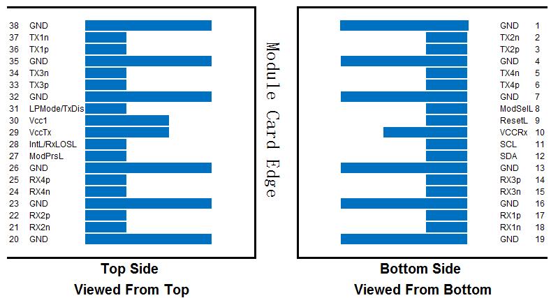
Figure 1. QSFP28-compliant 38-pin connector
Pin Function Definitions
| Pin | Symbols | Description | Notes |
|---|---|---|---|
| 1 | GND | Transmitter Ground (Common with Receiver Ground) | 1 |
| 2 | Tx2n | Transmitter Inverted Data Input | – |
| 3 | Tx2p | Transmitter Non-Inverted Data Input | – |
| 4 | GND | Transmitter Ground (Common with Receiver Ground) | 1 |
| 5 | Tx4n | Transmitter Inverted Data Input | – |
| 6 | Tx4p | Transmitter Non-Inverted Data Input | – |
| 7 | GND | Transmitter Ground (Common with Receiver Ground) | 1 |
| 8 | ModSelL | Module Select | – |
| 9 | ResetL | Module Reset | – |
| 10 | VccRx | 3.3V Power Supply Receiver | 2 |
| 11 | SCL | 2-Wire Serial Interface Clock | – |
| 12 | SDA | 2-Wire Serial Interface Data | – |
| 13 | GND | Transmitter Ground (Common with Receiver Ground) | 1 |
| 14 | Rx3p | Receiver Non-Inverted Data Output | – |
| 15 | Rx3n | Receiver Inverted Data Output | – |
| 16 | GND | Transmitter Ground (Common with Receiver Ground) | 1 |
| 17 | Rx1p | Receiver Non-Inverted Data Output | – |
| 18 | Rx1n | Receiver Inverted Data Output | 1 |
| 19 | GND | Transmitter Ground (Common with Receiver Ground) | 1 |
| 20 | GND | Transmitter Ground (Common with Receiver Ground) | – |
| 21 | Rx2n | Receiver Inverted Data Output | – |
| 22 | Rx2p | Receiver Non-Inverted Data Output | – |
| 23 | GND | Transmitter Ground (Common with Receiver Ground) | 1 |
| 24 | Rx4n | Receiver Inverted Data Output | – |
| 25 | Rx4p | Receiver Non-Inverted Data Output | – |
| 26 | GND | Transmitter Ground (Common with Receiver Ground) | 1 |
| 27 | ModPrsL | Module Present | – |
| 28 | IntL | Interrupt | – |
| 29 | VccTx | 3.3V Power Supply Transmitter | 2 |
| 30 | Vcc1 | 3.3V Power Supply | 2 |
| 31 | LPMode | Low Power Mode, not connect | – |
| 32 | GND | Transmitter Ground (Common with Receiver Ground) | 1 |
| 33 | Tx3p | Transmitter Non-Inverted Data Input | – |
| 34 | Tx3n | Transmitter Inverted Data Input | – |
| 35 | GND | Transmitter Ground (Common with Receiver Ground) | 1 |
| 36 | Tx1p | Transmitter Non-Inverted Data Input | – |
| 37 | Tx1n | Transmitter Inverted Data Input | – |
| 38 | GND | Transmitter Ground (Common with Receiver Ground) | 1 |
Notes:
- GND is the symbol for signal and supply (power) common for QSFP28 modules. All are common within the QSFP28 module and all module voltages are referenced to this potential unless otherwise noted. Connect these directly to the host board signal common ground plane.
- VccRx, Vcc1 and VccTx are the receiving and transmission power suppliers and shall be applied concurrently. Recommended host board power supply filtering is shown in the spec. VccRx, Vcc1 and VccTx may be internally connected within the QSFP28 transceiver module in any combination. The connector pins are each rated for a maximum current of 1000mA.
Mechanical Dimensions
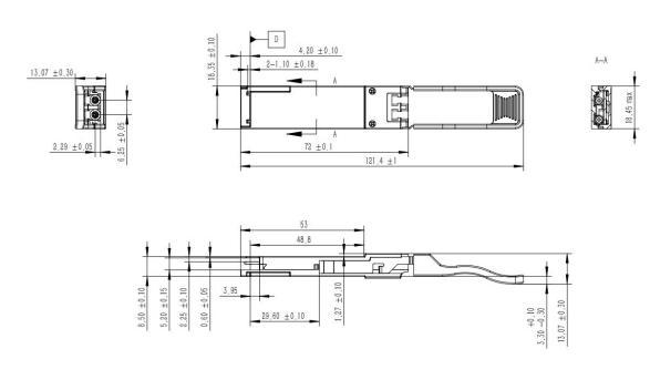
Figure 2. Mechanical dimensions
Ordering Information
| Part Number | Product Description |
|---|---|
| FTQ2-HG-SWDM4 | QSFP28, 100Gb/s, SWDM4, 0°C to 70°C |
本产品为【100G QSFP28 SWDM4 光收发模块】产品线,详细信息,请联系我们的销售人员,谢谢!
Important Notice
Performance figures, data and any illustrative material provided in this data sheet are typical and must be specifically confirmed in writing by F-tone Networks before they become applicable to any particular order or contract. In accordance with the F-tone Networks policy of continuous improvement specifications may change without notice.
The publication of information in this data sheet does not imply freedom from patent or other protective rights of F-tone Networks or others. Further details are available from any F-tone Networks sales representative.