
FTOA-4H-SR4 400G QSFP112 SR4 Transceiver
F-tone’s FTOA-4H-SR4 is a 400Gb/s QSFP112 optical module designed for 100m OM4/OM5 optical communication applications. On the transmitter side, the module converts 4 channels of 100Gb/s (PAM4) electrical input data to 4 channels of parallel optical signals, each capable of 100Gb/s operation for an aggregate data rate of 400Gb/s. On the receiver side, the module converts 4 channels of parallel optical signals of 100Gb/s each channel for an aggregate data rate of 400Gb/s into 4 channels of 100Gb/s (PAM4) electrical output data.
Product Features
- 400Gb/s multi-mode transceiver
- CMIS 5.0 compliance
- Power dissipation <9W
- Commercial case temperature range of 0°C to 70°C
- Single 3.3V power supply
- Maximum link length of 100m on OM4/OM5 and 60m on OM3
- Compliant with IEEE 802.3db
- 53.125GBd PAM4 × 4 channel VCSEL-based transmitter
- 53.125GBd PAM4 × 4 channel PIN receiver
- MPO-12/APC connector
- I²C management interface
Applications
- 1×400G Ethernet
- 2×200G Ethernet
- 4×100G Ethernet
- InfiniBand NDR
Regulatory Compliance
- ESD compatible with MIL-STD-883, Method 3015.4 / JESD22-A114-A (HBM)
- Laser Eye Safety compatible with FDA 21CFR 1040.10 and EN (IEC) 60825-1
- RoHS compliance
Transceiver Block Diagram
Pin Descriptions
| Pin | Symbol | Name | Notes |
|---|---|---|---|
| 1 | GND | Ground | 1 |
| 2 | Tx2n | Transmitter Inverted Data Input | |
| 3 | Tx2p | Transmitter Non-Inverted Data Input | |
| 4 | GND | Ground | 1 |
| 5 | Tx4n | Transmitter Inverted Data Input | |
| 6 | Tx4p | Transmitter Non-Inverted Data Input | |
| 7 | GND | Ground | 1 |
| 8 | ModSelL | Module Select | |
| 9 | ResetL | Module Reset | |
| 10 | VccRx | +3.3V Power Supply Receiver | 2 |
| 11 | SCL | 2-Wire Serial Interface Clock | |
| 12 | SDA | 2-Wire Serial Interface Data | |
| 13 | GND | Ground | 1 |
| 14 | Rx3p | Receiver Non-Inverted Data Output | |
| 15 | Rx3n | Receiver Inverted Data Output | |
| 16 | GND | Ground | 1 |
| 17 | Rx1p | Receiver Non-Inverted Data Output | |
| 18 | Rx1n | Receiver Inverted Data Output | |
| 19 | GND | Ground | 1 |
| 20 | GND | Ground | 1 |
| 21 | Rx2n | Receiver Inverted Data Output | |
| 22 | Rx2p | Receiver Non-Inverted Data Output | |
| 23 | GND | Ground | 1 |
| 24 | Rx4n | Receiver Inverted Data Output | |
| 25 | Rx4p | Receiver Non-Inverted Data Output | |
| 26 | GND | Ground | 1 |
| 27 | ModPrsL | Module Present | |
| 28 | IntL/RxLOS | Interrupt / optional RxLOS | |
| 29 | VccTx | +3.3V Power Supply Transmitter | 2 |
| 30 | Vcc1 | +3.3V Power Supply | 2 |
| 31 | LPMode/TxDis | Low Power Mode / optional Tx Disable | |
| 32 | GND | Ground | 1 |
| 33 | Tx3p | Transmitter Non-Inverted Data Input | |
| 34 | Tx3n | Transmitter Inverted Data Input | |
| 35 | GND | Ground | 1 |
| 36 | Tx1p | Transmitter Non-Inverted Data Input | |
| 37 | Tx1n | Transmitter Inverted Data Input | |
| 38 | GND | Ground | 1 |
Notes:
- Note 1: GND is the symbol for signal and supply (power) common for the QSFP112 module. All are common within the QSFP112 module and all voltages are referenced to this potential unless otherwise noted. Connect these directly to the host board signal-common ground plane.
- Note 2: VccRx, Vcc1 and VccTx are the receiver and transmitter power supplies and shall be applied concurrently. VccRx, Vcc1 and VccTx may be internally connected within the QSFP112 module in any combination. The connector pins are each rated for a maximum current of 1.5A (max. current of 2.0A is required for high module power of 15-20W).
Absolute Maximum Ratings
| Parameter | Symbol | Min | Typ | Max | Unit | Notes |
|---|---|---|---|---|---|---|
| Storage Temperature | Tstg | -40 | +85 | °C | ||
| Supply Voltage | VCC | -0.5 | 3.5 | V | ||
| Operating Relative Humidity | RH | 0 | 85 | % | Non-condensing |
Recommended Operating Conditions
| Parameter | Symbol | Min | Typ | Max | Unit | Notes |
|---|---|---|---|---|---|---|
| Case Operating Temperature | Tc | 0 | +70 | °C | ||
| Power Supply Voltage | Vcc | 3.135 | 3.3 | +3.465 | V | |
| Module Power Dissipation | P | 9 | W |
Electrical Characteristics
| Parameter | Symbol | Min | Typ | Max | Unit | Notes |
|---|---|---|---|---|---|---|
| Transmitter | ||||||
| Differential Input Voltage Peak to Peak Swing | VIpp | 600 | 845 | mV | ||
| Differential Input Impedance | ZIN | 90 | 100 | 110 | Ω | |
| Receiver | ||||||
| Differential Output Voltage Peak to Peak Swing | Vopp | 600 | 845 | mV | ||
| Differential Output Impedance | Zout | 90 | 100 | 110 | Ω | |
Optical Characteristics
Transmitter
| Parameter | Symbol | Min | Typ | Max | Unit | Notes |
|---|---|---|---|---|---|---|
| Data Rate, each Lane | 53.125±100ppm | GBd | ||||
| Modulation Format | PAM4 | |||||
| Center Wavelength | λc | 844 | 863 | nm | ||
| RMS spectral width | 0.6 | nm | 1 | |||
| Average Launch Power, each Lane | PAVG | -4.6 | 4 | dBm | 2 | |
| Outer Optical Modulation Amplitude (OMAouter), each Lane max – For max(TECQ, TDECQ) ≤ 1.8dB | POMA | -2.6 | 3.5 | dBm | ||
| Outer Optical Modulation Amplitude (OMAouter), each Lane max – For 1.8 < max(TECQ, TDECQ) ≤ 4.4dB | POMA | -4.4+max(TECQ, TDECQ) | 3.5 | dBm | ||
| TDECQ, each Lane | TDECQ | 4.4 | dB | |||
| Transmitter eye closure for PAM4, each lane | TECQ | 4.4 | dB | |||
| Overshoot/undershoot | 29 | % | ||||
| Extinction Ratio | ER | 2.5 | dB | |||
| Transmitter Transition Time | 17 | ps | ||||
| Average launch power of OFF transmitter | Toff | -30 | dBm | |||
| RIN14OMA | RIN | -132 | dB/Hz | |||
| Optical Return Loss Tolerance | ORLT | 14 | dB | |||
| Encircled flux | ≥86% at 19μm; ≤30% at 4.5μm | 3 | ||||
Receiver
| Parameter | Symbol | Min | Typ | Max | Unit | Notes |
|---|---|---|---|---|---|---|
| Data Rate, each Lane | 53.125±100ppm | GBd | ||||
| Modulation Format | PAM4 | |||||
| Center wavelength | λc | 842 | 948 | nm | ||
| Damage Threshold, each Lane | 5 | dBm | 4 | |||
| Average Receive Power, each Lane | -6.4 | 4 | dBm | 5 | ||
| Receive Power (OMAouter), each Lane | 3.5 | dBm | ||||
| Receiver Sensitivity (OMAouter) – For TECQ ≤ 1.8dB | SEN | -4.6 | dBm | |||
| Receiver Sensitivity (OMAouter) – For 1.8 < TECQ ≤ 4.4dB | SEN | -6.4+TECQ | dBm | |||
| Stressed Receiver Sensitivity (OMAouter), each Lane | SRS | -2 | dBm | 6 | ||
| Receiver Reflectance | -15 | dB | ||||
| LOS Assert | LOSA | -17 | dBm | |||
| LOS De-assert | LOSD | -8 | dBm | |||
| LOS Hysteresis | LOSH | 0.5 | dB | |||
Conditions of Stressed Receiver Sensitivity Test
| Parameter | Min | Typ | Max | Unit | Notes |
|---|---|---|---|---|---|
| Stressed Eye Closure for PAM4 (SECQ), Lane under Test | 4.4 | dB | 7 | ||
| OMAouter of each aggressor lane | 3.5 | dBm |
Notes
- Note 1: RMS spectral width is the standard deviation of the spectrum.
- Note 2: Average launch power, each lane (min) is informative and not the principal indicator of signal strength. A transmitter with launch power below this value cannot be compliant; however, a value above this does not ensure compliance.
- Note 3: If measured in to type A1a.2 or type A1a.3, or A1a.4, 50μm fiber, in accordance with IEC 61280-1-4.
- Note 4: The receiver shall be able to tolerate, without damage, continuous exposure to a modulated optical input signal having this power level on one lane. The receiver does not have to operate correctly at this input power.
- Note 5: Average receive power, each lane (min) is informative and not the principal indicator of signal strength. A received power below this value cannot be compliant; however, a value above this does not ensure compliance.
- Note 6: Measured with conformance test signal at TP3 for the BER equal to 2.4×10⁻⁴.
- Note 7: These test conditions are for measuring stressed receiver sensitivity. They are not characteristics of the receiver.
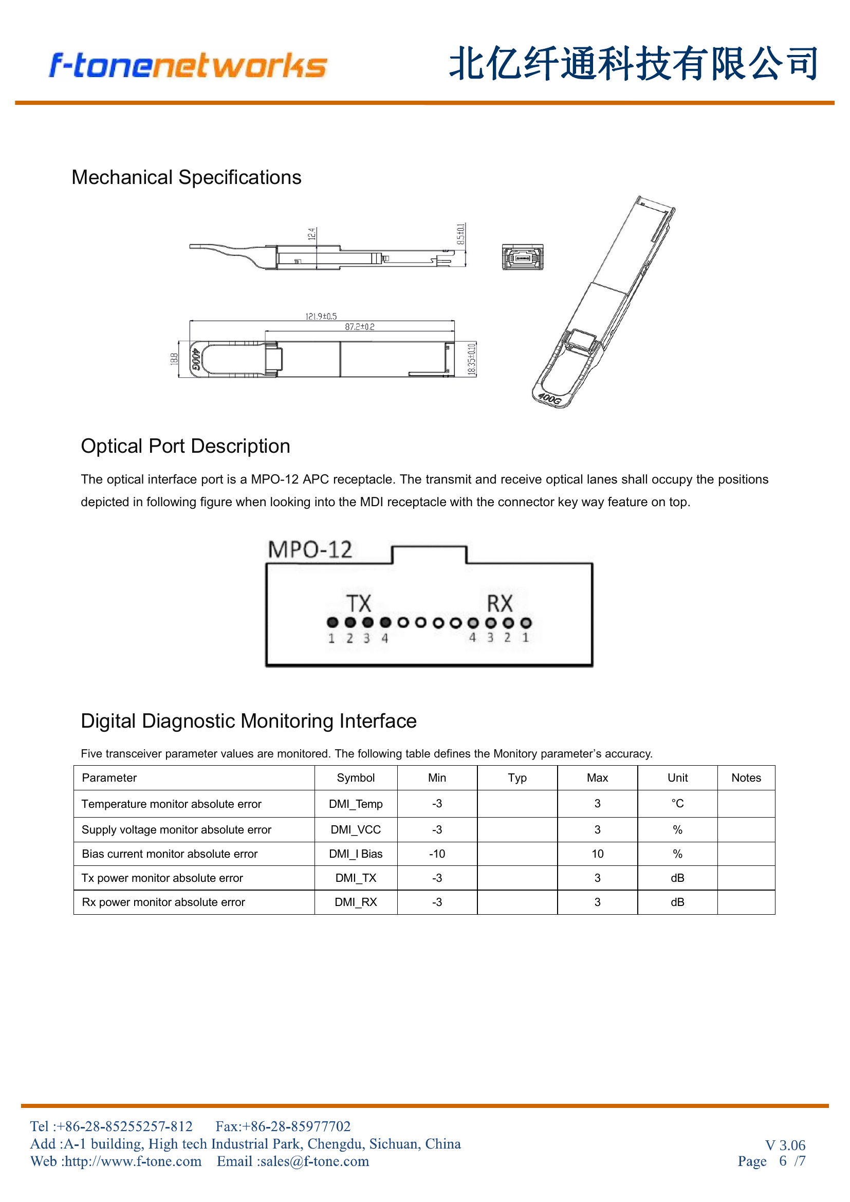
Mechanical Specifications
Optical Port Description
The optical interface port is a MPO-12 APC receptacle. The transmit and receive optical lanes shall occupy the positions depicted when looking into the MDI receptacle with the connector keyway feature on top.
Digital Diagnostic Monitoring Interface
Five transceiver parameter values are monitored. The following table defines the monitor parameter’s accuracy.