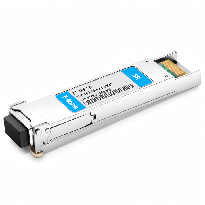
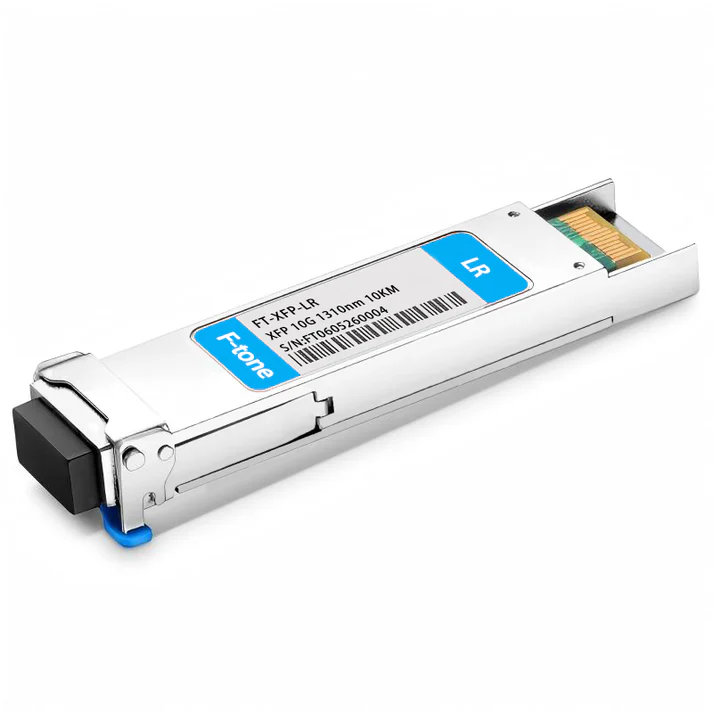
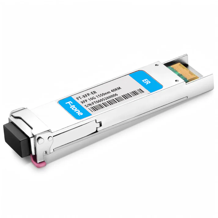
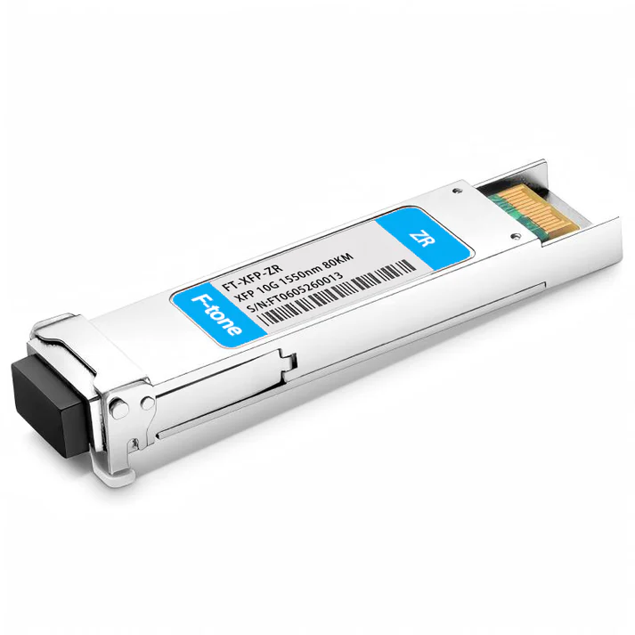
FTCX-Dxx1X-40Dxx 10Gb/s XFP DWDM 40km 光收发器
Features
- Up to 11.3Gb/s data links
- DWDM EML transmitter and PIN receiver
- 100 GHz ITU channel spacing with integrated wavelength locker
- Up to 40km on 9/125µm SMF
- Hot-pluggable XFP footprint
- Duplex LC/UPC type pluggable optical interface
- RoHS-10 compliant and lead-free
- Support Digital Monitoring interface
- Single +3.3V power supply
- Maximum power consumption 1.8W
- Metal enclosure, for lower EMI
- Meet ESD requirements, resist 8KV direct contact voltage
- Case operating temperature: Commercial 0~+70°C, Extended -10~+80°C, Industrial -40~+85°C
Applications
- 10GBASE-ER/EW & 10G Ethernet
- SONET OC-192 & SDH STM I-64.1
- 10G Fiber Channel
General Description
F-tone FTCX-Dxx1X-40Dxx XFP transceiver is designed for use in 10-Gigabit Ethernet links up to 40km over single mode fiber. The module consists of DWDM EML Laser, PIN and Preamplifier in a high-integrated optical sub-assembly. Digital diagnostics functions are available via a 2-wire serial interface, as specified in XFP MSA. This module is designed for single mode fiber and operates at a nominal wavelength of 100GHz ITU Grid, C Band DWDM wavelength.
The transceivers provide enhanced digital diagnostic monitoring interface, which allows real-time access to device operating parameters such as transceiver temperature, laser bias current, transmitted optical power, and received optical power and transceiver supply voltage. It also defines a sophisticated system of alarm and warning flags, which alerts end-users when particular operating parameters are outside of a factory set normal range.
Absolute Maximum Ratings
| Parameter | Symbol | Min | Max | Unit | Notes |
|---|---|---|---|---|---|
| Storage Temperature | TS | -40 | 85 | °C | |
| Power Supply Voltage | VCC | -0.5 | 3.6 | V | |
| Relative Humidity | RH | 5 | 95 | % | non-condensation |
| Damage Threshold | Td | – | 5 | dBm |
Recommended Operating Conditions
| Parameter | Symbol | Min | Typical | Max | Unit | Notes |
|---|---|---|---|---|---|---|
| Operating Case Temperature (Commercial) | TOP | 0 | – | 70 | °C | |
| Operating Case Temperature (Extended) | TOP | -10 | – | 80 | °C | |
| Operating Case Temperature (Industrial) | TOP | -40 | – | 85 | °C | |
| Power Supply Voltage | VCC | 3.135 | 3.3 | 3.465 | V | |
| Data Rate | – | – | 10.3125 | – | Gb/s | |
| Control Input Voltage High | – | 2 | – | Vcc | V | |
| Control Input Voltage Low | – | 0 | – | 0.8 | V | |
| Link Distance (SMF) | D | – | 40 | – | km | 9/125µm |
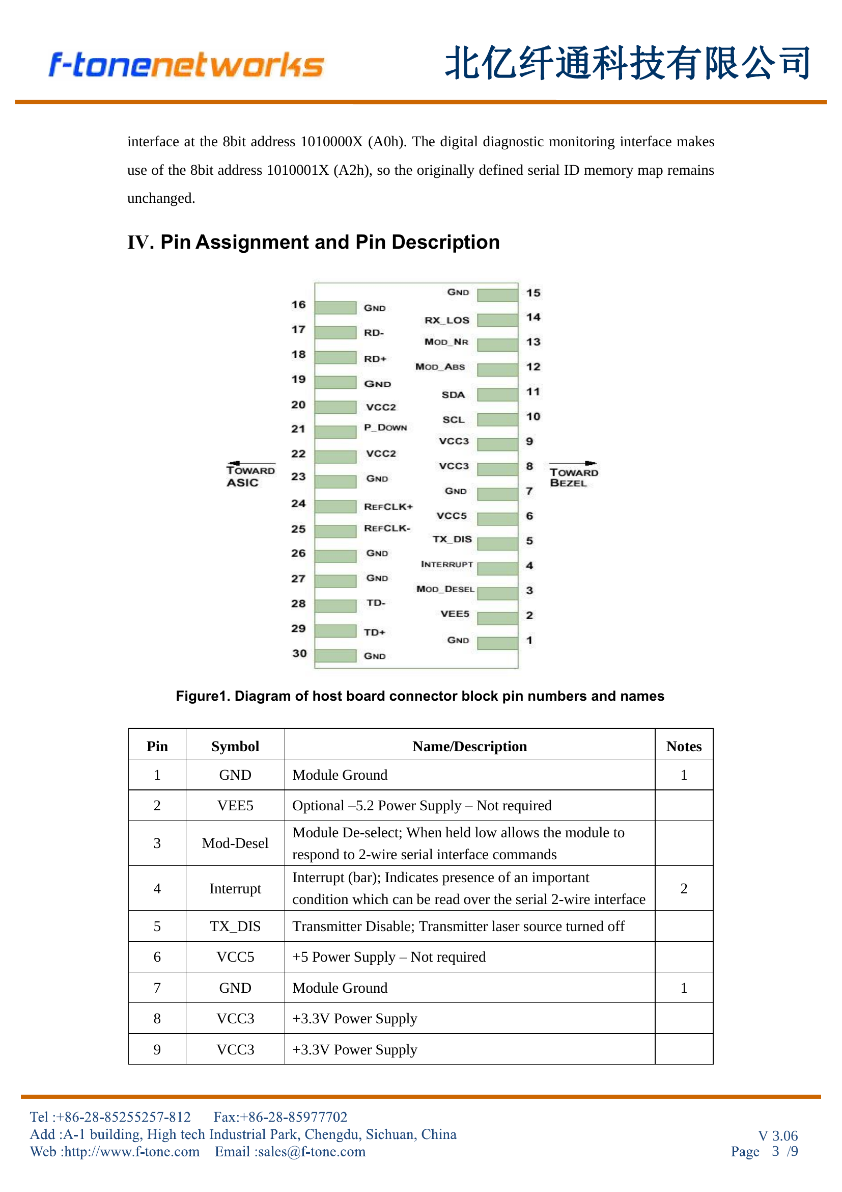
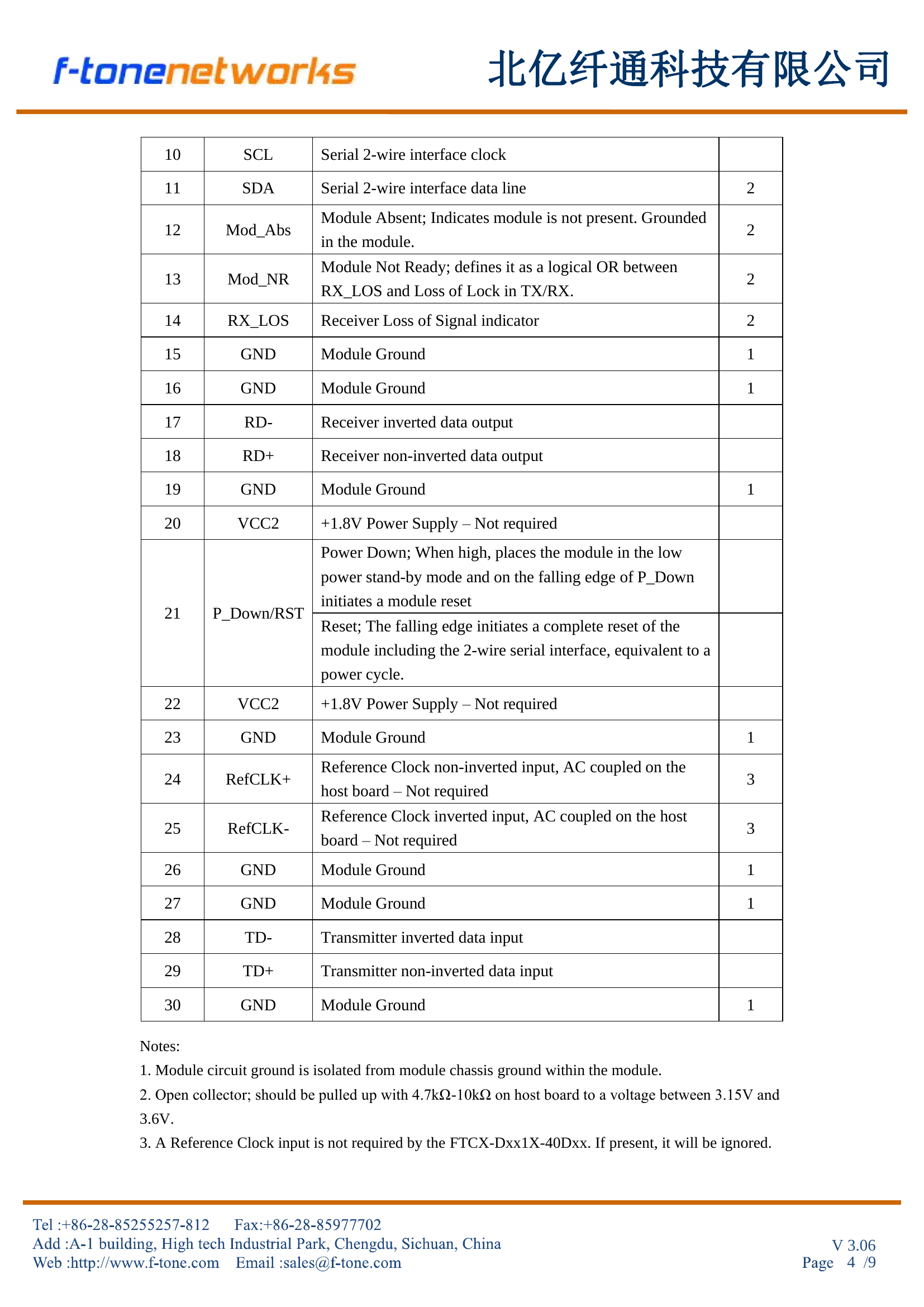
Pin Description
| Pin | Symbol | Name/Description | Notes |
|---|---|---|---|
| 1 | GND | Module Ground | 1 |
| 3 | Mod-Desel | Module De-select (low = active) | |
| 4 | Interrupt | Interrupt indicator via serial interface | 2 |
| 5 | TX_DIS | Transmitter Disable | |
| 8-9 | VCC3 | +3.3V Power Supply | |
| 10 | SCL | Serial 2-wire interface clock | |
| 11 | SDA | Serial 2-wire interface data line | 2 |
| 12 | Mod_Abs | Module Absent (grounded in module) | 2 |
| 13 | Mod_NR | Module Not Ready (RX_LOS OR Loss of Lock) | 2 |
| 14 | RX_LOS | Receiver Loss of Signal indicator | 2 |
| 17 | RD- | Receiver inverted data output | |
| 18 | RD+ | Receiver non-inverted data output | |
| 21 | P_Down/RST | Power Down / Reset | |
| 28 | TD- | Transmitter inverted data input | |
| 29 | TD+ | Transmitter non-inverted data input |
Notes:
1. Module circuit ground is isolated from module chassis ground.
2. Open collector; pulled up with 4.7kΩ-10kΩ on host board to 3.15V~3.6V.
3. Reference Clock input not required by FTCX-Dxx1X-40Dxx.
Electrical Characteristics
| Parameter | Symbol | Min | Typ | Max | Unit | Notes |
|---|---|---|---|---|---|---|
| Power Consumption | P | – | – | 1.8 | W | |
| Supply Current | Icc | – | – | 520 | mA | |
| TX Input Voltage Tolerance | – | Vcc-0.3 | – | 4.0 | V | |
| TX AC Common Mode Voltage | – | – | – | 15 | mV | RMS |
| TX Differential Input Voltage Swing | Vin,pp | 120 | – | 820 | mVpp | |
| TX Differential Input Impedance | Zin | 90 | 100 | 110 | Ω | 1 |
| Tx Disable Assert Time | – | – | – | 10 | µs | |
| TX Disable Voltage | Vdis | Vcc-1.3 | – | Vcc | V | |
| TX Enable Voltage | Ven | Vee | – | Vee+0.8 | V | 2 |
| RX Differential Output Swing | Vout,pp | 350 | – | 850 | mVpp | |
| RX Differential Output Impedance | Zout | 90 | 100 | 110 | Ω | 3 |
| Data Output Rise/Fall Time | Tr/Tf | – | 28 | – | ps | 4 |
| LOS Assert Voltage | VlosH | Vcc-1.3 | – | Vcc | V | 5 |
| LOS De-assert Voltage | VlosL | Vee | – | Vee+0.8 | V | 5 |
| Power Supply Rejection | PSR | – | – | 100 | mVpp | 6 |
Notes:
1. Connected directly to TX data input pins, AC coupled thereafter.
2. Or open circuit.
3. Input 100 ohms differential termination.
4. Unfiltered 20-80% values.
5. LVTTL logic: 0 = normal, 1 = no signal.
6. Receiver sensitivity compliant with power supply sinusoidal modulation 20Hz-1.5MHz.
Optical Characteristics
Transmitter
| Parameter | Symbol | Min | Typ | Max | Unit | Notes |
|---|---|---|---|---|---|---|
| Optical Wavelength | λc | λc-0.1 | – | λc+0.1 | nm | 1 |
| Center Wavelength Spacing | – | – | 100 | – | GHz | |
| Optical Spectral Width | Δλ | – | – | 1 | nm | |
| Side Mode Suppression Ratio | SMSR | 30 | – | – | dB | |
| Average Optical Power | PAVG | 0 | – | 4 | dBm | 2 |
| Optical Extinction Ratio | ER | 8.2 | – | – | dB | |
| Transmitter and Dispersion Penalty | TDP | – | – | 3 | dB | |
| TX OFF Output Power | POff | – | – | -30 | dBm | |
| Transmitter Eye Mask | – | Compliant with IEEE802.3ae | – | |||
Receiver
| Parameter | Symbol | Min | Typ | Max | Unit | Notes |
|---|---|---|---|---|---|---|
| Center Wavelength | λ | 1270 | – | 1610 | nm | |
| Receiver Sensitivity | Sen. | – | – | -16.5 | dBm | 3 |
| Input Saturation Power | Psat | – | – | 0.5 | dBm | |
| LOS Assert | LOSA | – | – | -32 | dBm | |
| LOS De-assert | LOSD | – | – | -18 | dBm | |
| LOS Hysteresis | LOSH | – | 0.5 | – | dBm |
Notes:
1. λc refers to wavelength selection, corresponds to approximately 0.8nm.
2. Class 1 Laser Safety per FDA/CDRH and IEC-825-1.
3. Measured with 1528.77~1563.86nm source, ER=8.2dB; BER≤1E-12 @10.3125Gbps, PRBS=2³¹-1 NRZ.
Digital Diagnostic Functions
| Parameter | Symbol | Min | Max | Unit | Notes |
|---|---|---|---|---|---|
| Temperature Monitor Error | DMI_Temp | -3 | 3 | °C | Over operating temp |
| Supply Voltage Monitor Error | DMI_VCC | -0.15 | 0.15 | V | Full operating range |
| RX Power Monitor Error | DMI_RX | -3 | 3 | dB | |
| Bias Current Monitor | DMI_bias | -10% | 10% | mA | |
| TX Power Monitor Error | DMI_TX | -3 | 3 | dB |
Mechanical Dimensions
Ordering Information
| Part Number | Data Rate (Gb/s) | Wavelength (nm) | Distance (km) | Temperature (°C) |
|---|---|---|---|---|
| FTCX-Dxx1X-40D | 10.3125 | Refer to wavelength selection | 40 | 0~70 (Commercial) |
| FTCX-Dxx1X-40DE | 10.3125 | 40 | -10~80 (Extended) | |
| FTCX-Dxx1X-40DI | 10.3125 | 40 | -40~85 (Industrial) |
λC Wavelength Guide (100GHz ITU C-Band)
| Ch (xx) | λ (nm) | Freq (THz) | Ch (xx) | λ (nm) | Freq (THz) |
|---|---|---|---|---|---|
| 17 | 1563.86 | 191.70 | 39 | 1546.12 | 193.90 |
| 18 | 1563.05 | 191.80 | 40 | 1545.32 | 194.00 |
| 19 | 1562.23 | 191.90 | 41 | 1544.53 | 194.10 |
| 20 | 1561.42 | 192.00 | 42 | 1543.73 | 194.20 |
| 21 | 1560.61 | 192.10 | 43 | 1542.94 | 194.30 |
| 22 | 1559.79 | 192.20 | 44 | 1542.14 | 194.40 |
| 23 | 1558.98 | 192.30 | 45 | 1541.35 | 194.50 |
| 24 | 1558.17 | 192.40 | 46 | 1540.56 | 194.60 |
| 25 | 1557.36 | 192.50 | 47 | 1539.77 | 194.70 |
| 26 | 1556.55 | 192.60 | 48 | 1538.98 | 194.80 |
| 27 | 1555.75 | 192.70 | 49 | 1538.19 | 194.90 |
| 28 | 1554.94 | 192.80 | 50 | 1537.40 | 195.00 |
| 29 | 1554.13 | 192.90 | 51 | 1536.61 | 195.10 |
| 30 | 1553.33 | 193.00 | 52 | 1535.82 | 195.20 |
| 31 | 1552.52 | 193.10 | 53 | 1535.04 | 195.30 |
| 32 | 1551.72 | 193.20 | 54 | 1534.25 | 195.40 |
| 33 | 1550.92 | 193.30 | 55 | 1533.47 | 195.50 |
| 34 | 1550.12 | 193.40 | 56 | 1532.68 | 195.60 |
| 35 | 1549.32 | 193.50 | 57 | 1531.90 | 195.70 |
| 36 | 1548.51 | 193.60 | 58 | 1531.12 | 195.80 |
| 37 | 1547.72 | 193.70 | 59 | 1530.33
|