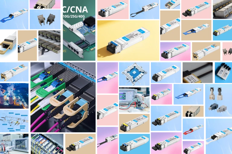
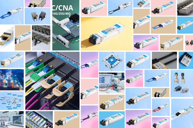
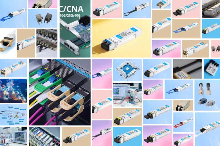
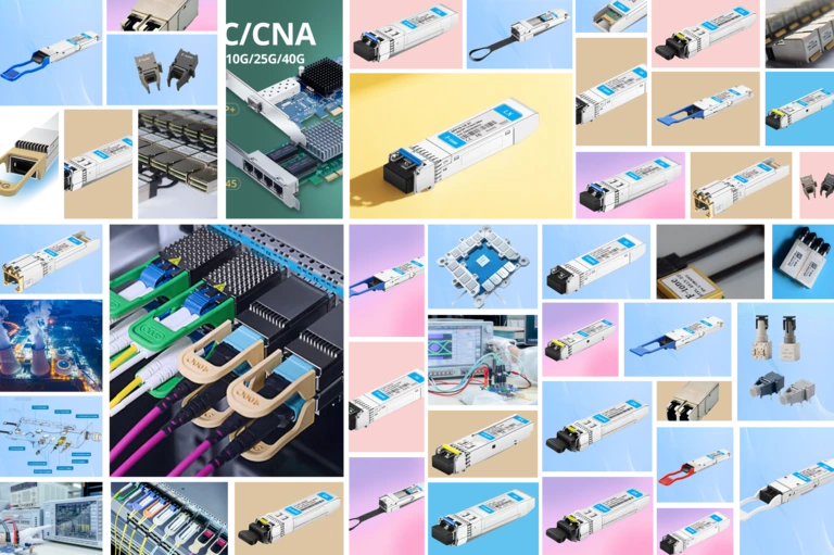
FTQD-2H-LR8 200G QSFPDD LR8 Optical Transceiver Module — The F-tone Networks FTQD-2H-LR8 is an Eight-Channel, Pluggable, Fiber-Optic QSFP DD LR8 for 2×100 Gigabit Ethernet Applications. It integrates eight data lanes in each direction with 208Gbps bandwidth. Each lane can operate at 26Gbps up to 10km over G.652 SMF using LAN-WDM 8 wavelengths.
Module Block Diagram
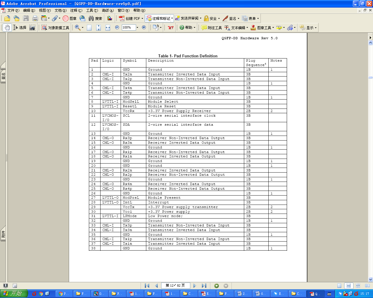
Figure 1. Module Block Diagram
Features
- 8 channels full-duplex transceiver modules
- Transmission data rate up to 26Gbps per channel
- 8 x 26Gb/s DFB-based LAN-WDM Cooling transmitter
- 8 channels PIN ROSA
- Internal CDR circuits on both receiver and transmitter channels
- Support CDR bypass
- Low power consumption <7.5W
- Hot Pluggable QSFP DD form factor and Compliant with CMIS
- Up to 10km reach for G.652 SMF
- Duplex LC receptacles
- Built-in digital diagnostic functions
- Operating case temperature 0°C to +70°C
- 3.3V power supply voltage
- RoHS 6 compliant (lead free)
Applications
- IEEE 802.3ba 100GBASE-LR4
Absolute Maximum Ratings
| Parameter | Symbol | Min | Max | Unit |
|---|---|---|---|---|
| Supply Voltage | Vcc | -0.3 | 3.6 | V |
| Input Voltage | Vin | -0.3 | Vcc+0.3 | V |
| Storage Temperature | Tst | -20 | 85 | °C |
| Case Operating Temperature | Top | 0 | 70 | °C |
| Humidity (non-condensing) | Rh | 5 | 95 | % |
Recommended Operating Conditions
| Parameter | Symbol | Min | Typical | Max | Unit |
|---|---|---|---|---|---|
| Supply Voltage | Vcc | 3.13 | 3.3 | 3.47 | V |
| Operating Case Temperature | Tc | 0 | – | 70 | °C |
| Data Rate Per Lane | fd | – | 25.78125 | – | Gbps |
| Humidity | Rh | 5 | – | 85 | % |
| Power Dissipation | Pm | – | – | 7.5 | W |
| Fiber Bend Radius | Rb | 0.002 | – | 10 | km |
Electrical Specifications
(Ambient Operating Temperature Ta=+25±5°C)
| Parameter | Symbol | Min | Typical | Max | Unit |
|---|---|---|---|---|---|
| Differential Input Impedance | Zin | 90 | 100 | 110 | ohm |
| Differential Output Impedance | Zout | 90 | 100 | 110 | ohm |
| Differential Input Voltage Amplitude | ΔVin | 190 | – | 700 | mVp-p |
| Differential Output Voltage Amplitude | ΔVout | 300 | – | 850 | mVp-p |
| Input Logic Level High | VIH | 2.0 | – | Vcc | V |
| Input Logic Level Low | VIL | 0 | – | 0.8 | V |
| Output Logic Level High | VOH | Vcc-0.5 | – | Vcc | V |
| Output Logic Level Low | VOL | 0 | – | 0.4 | V |
Note: Differential input/output voltage amplitude is measured between TxnP/TxnN and RxnP/RxnN respectively.
Optical Characteristics
Table 3 — 100GBASE-LR4 Optical Characteristics
| Parameter | Symbol | Min | Typical | Max | Unit | Notes |
|---|---|---|---|---|---|---|
| Lane Wavelength L0 | λL0 | 1272.55 | 1273.54 | 1274.54 | nm | |
| Lane Wavelength L1 | λL1 | 1276.89 | 1277.89 | 1278.89 | nm | |
| Lane Wavelength L2 | λL2 | 1281.25 | 1282.26 | 1283.27 | nm | |
| Lane Wavelength L3 | λL3 | 1285.65 | 1286.66 | 1287.68 | nm | |
| Lane Wavelength L4 | λL4 | 1294.53 | 1295.56 | 1296.59 | nm | |
| Lane Wavelength L5 | λL5 | 1299.02 | 1300.05 | 1301.09 | nm | |
| Lane Wavelength L6 | λL6 | 1303.54 | 1304.58 | 1305.63 | nm | |
| Lane Wavelength L7 | λL7 | 1308.09 | 1309.14 | 1310.19 | nm | |
| SMSR | SMSR | 30 | – | – | dB | |
| Total Average Launch Power | PT | – | – | 10.5 | dBm | |
| Average Launch Power, each Lane | PAVG | -4.3 | – | 4.5 | dBm | |
| OMA, each Lane | POMA | -1.3 | – | 4.5 | dBm | 1 |
| Difference in Launch Power between any Two Lanes (OMA) | Ptx,diff | – | – | 5 | dB | |
| Launch Power in OMA minus TDP, each Lane | – | -2.3 | – | – | dBm | |
| TDP, each Lane | TDP | – | – | 2.2 | dB | |
| Extinction Ratio | ER | 4 | – | – | dB | |
| RIN20OMA | RIN | – | – | -130 | dB/Hz | |
| Optical Return Loss Tolerance | TOL | – | – | 20 | dB | |
| Transmitter Reflectance | RT | – | – | -12 | dB | |
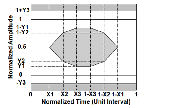
| Eye Mask coordinates: X1,X2,X3,Y1,Y2,Y3 | – | {0.25, 0.4, 0.45, 0.25, 0.28, 0.4} | – | {0.25, 0.4, 0.45, 0.25, 0.28, 0.4} | 2 | |
| Average Launch Power OFF Transmitter, each Lane | Poff | – | – | -30 | dBm | |
| Damage Threshold, each Lane | THd | 5.5 | – | – | dBm | 3 |
| Total Average Receive Power | – | – | – | 10.5 | dBm | |
| Average Receive Power, each Lane | – | -10.6 | – | 4.5 | dBm | |
| Receive Power (OMA), each Lane | – | – | – | 4.5 | dBm | |
| Receiver Sensitivity (OMA), each Lane | SEN | – | – | -8.6 | dBm | |
| Stressed Receiver Sensitivity (OMA), each Lane | – | – | – | -6.8 | dBm | 4 |
| Difference in Receive Power between any Two Lanes (OMA) | Prx,diff | – | – | 5.5 | dB | |
| LOS Assert | LOSA | – | -18 | – | dBm | |
| LOS Deassert | LOSD | – | -15 | – | dBm | |
| LOS Hysteresis | LOSH | 0.5 | – | – | dB | |
| Receiver Electrical 3 dB Upper Cutoff Frequency, each Lane | Fc | – | – | 31 | GHz | |
| Vertical Eye Closure Penalty, each Lane | – | – | 1.8 | – | dB | 5 |
| Stressed Eye J2 Jitter, each Lane | – | – | 0.3 | – | UI | |
| Stressed Eye J9 Jitter, each Lane | – | – | 0.47 | – | UI |
Notes: 1. Even if TDP < 1 dB, the OMA min must exceed the minimum value. 2. Eye mask coordinates. 3. Continuous exposure without damage; receiver does not have to operate correctly. 4. Measured with conformance test signal at BER=1×10⁻¹². 5. Vertical eye closure penalty and stressed eye jitter are test conditions for stressed receiver sensitivity.
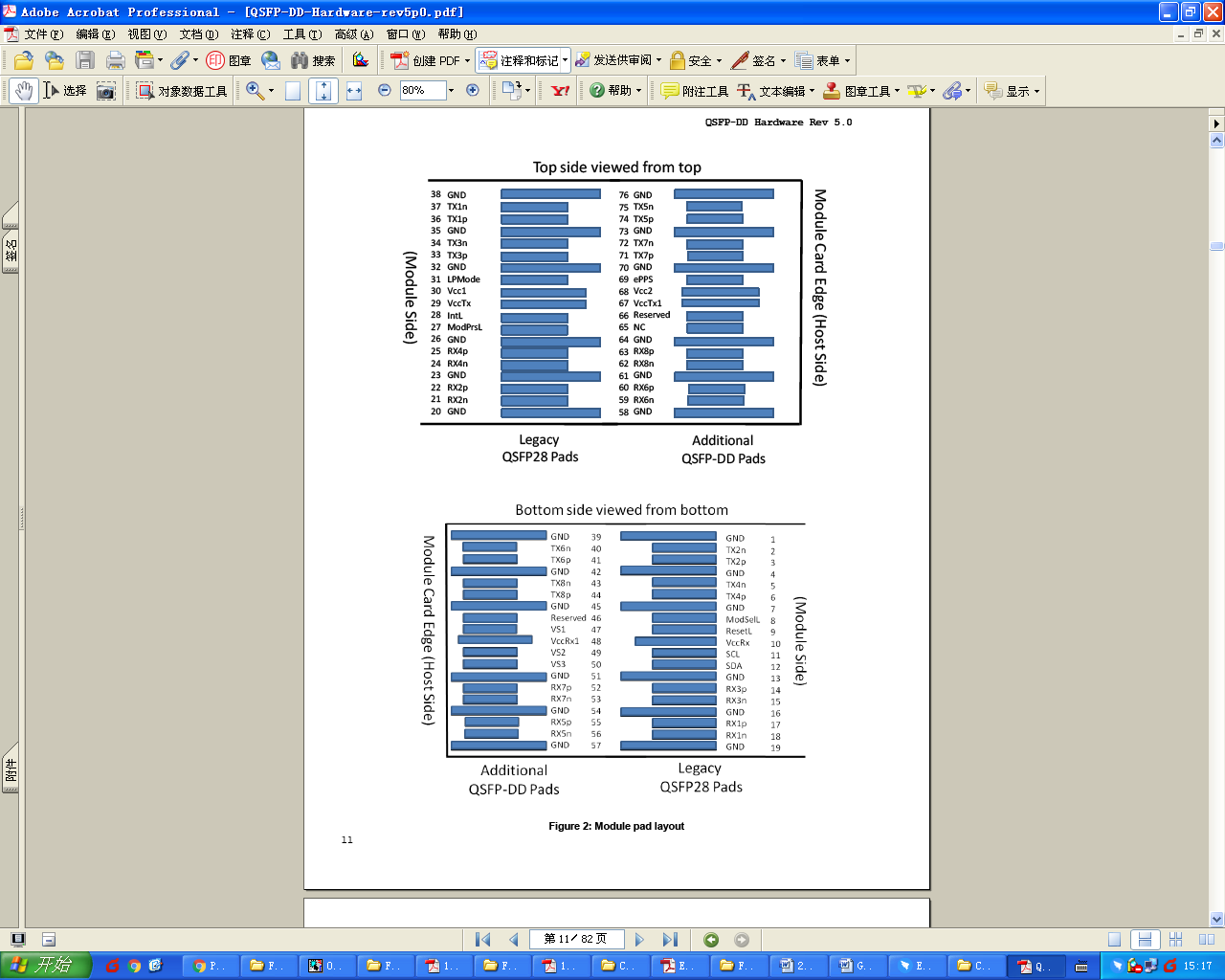
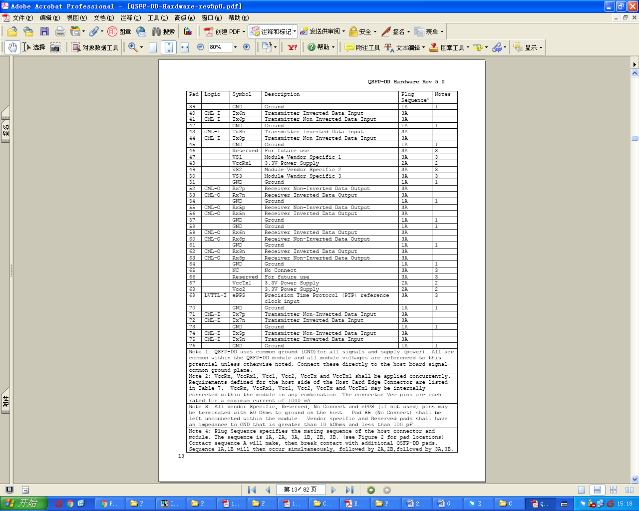
Pin Description
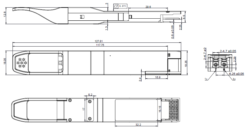
Figure 2. Electrical Pin-out Details
ModSelL Pin
The ModSelL is an input signal pulled to Vcc in the QSFP-DD module. When held low by the host, the module responds to 2-wire serial communication commands. Allows multiple QSFP-DD modules on a single 2-wire interface bus.
ResetL Pin
The ResetL signal is pulled to Vcc in the module. A low level for longer than the minimum pulse length initiates a complete module reset, returning all user settings to default state.
LPMode Pin
LPMode is an input signal pulled up to Vcc in the QSFP-DD module. Used in the control of module power mode (See CMIS Section 6.3.1.3).
ModPrsL Pin
ModPrsL is pulled up to Vcc on the host board and grounded in the module. Asserted “Low” when module is inserted, deasserted “High” when physically absent.
IntL Pin
IntL is an open collector output, pulled to Vcc on the host board. When asserted Low, it indicates a change in module state, a possible operational fault, or a status critical to the host system.
Power Supply Filtering
The host board should use the power supply filtering shown below.
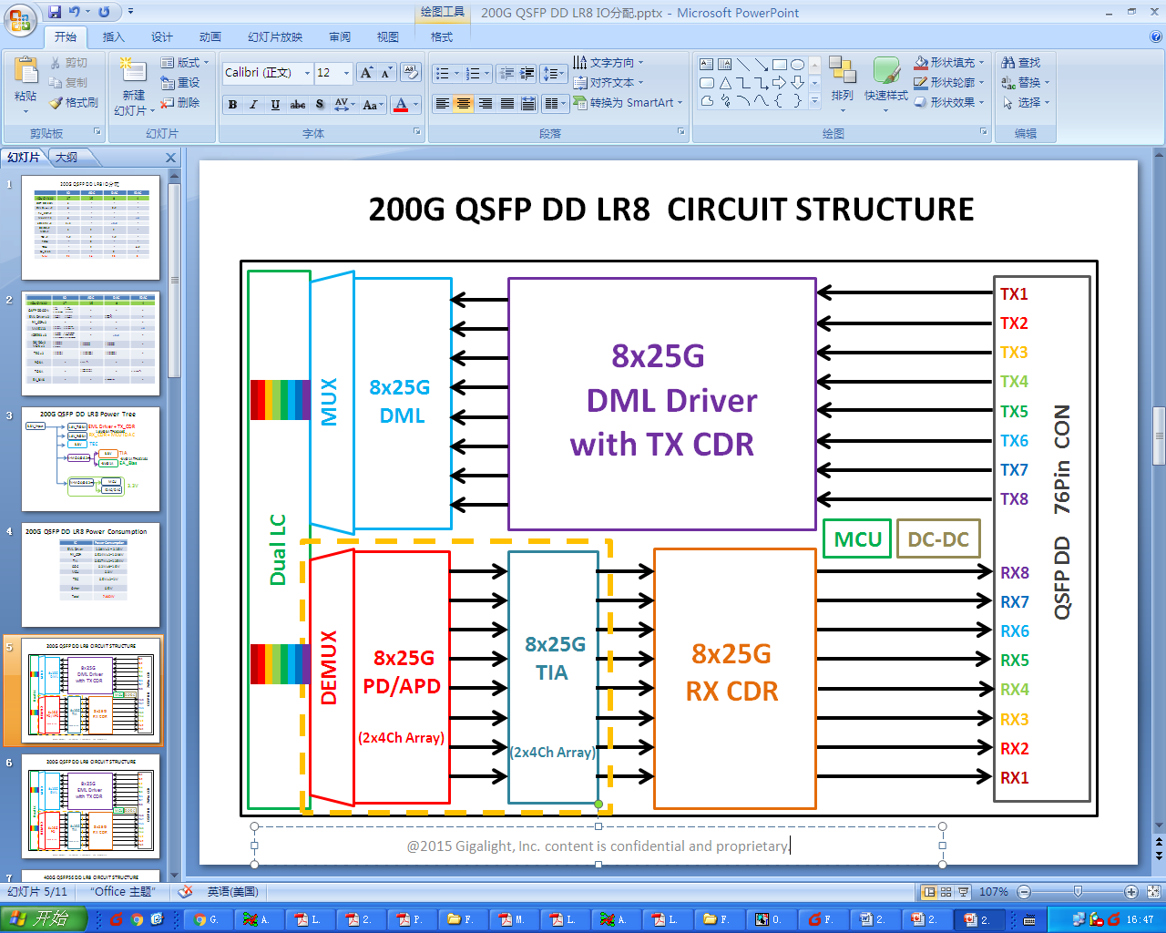
Figure 3. Host Board Power Supply Filtering
Diagnostic Monitoring Interface
Digital diagnostics monitoring is available on all F-tone Networks QSFP DD products. A 2-wire serial interface provides user contact with the module. The CMIS Memory Map defines serial ID, digital monitoring, and control functions.
The memory space is arranged into a lower single-page address space of 128 bytes and multiple upper address space pages. This structure supports a flat 256 byte memory for passive copper cables and permits timely access to addresses in the lower page (Flags and Monitors). Less time critical entries (serial ID, threshold settings) use the Page Select function.
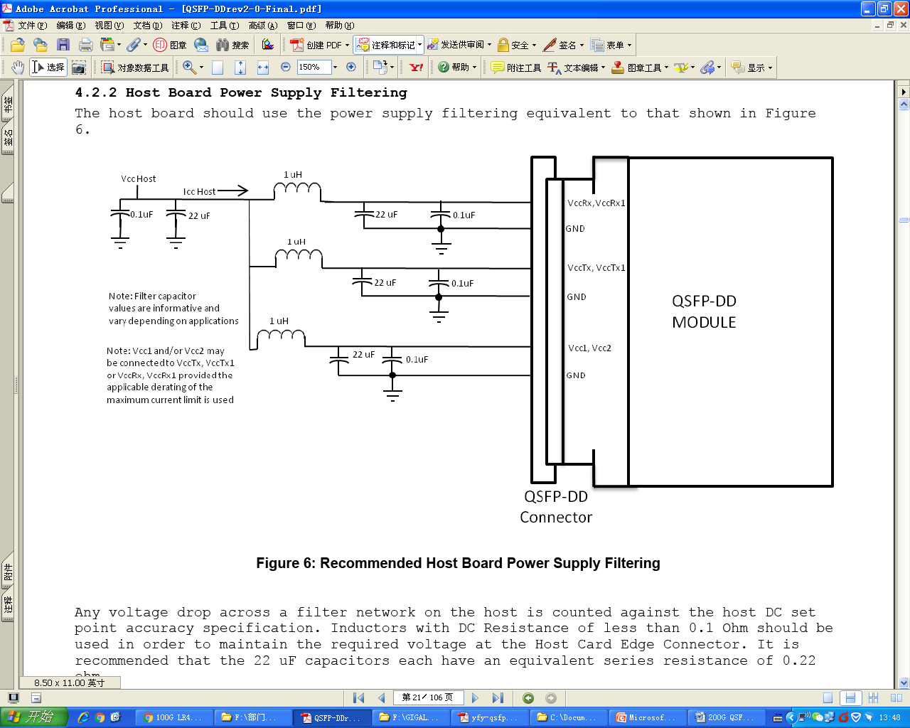
Figure 4. QSFP DD Memory Map
Mechanical Dimensions
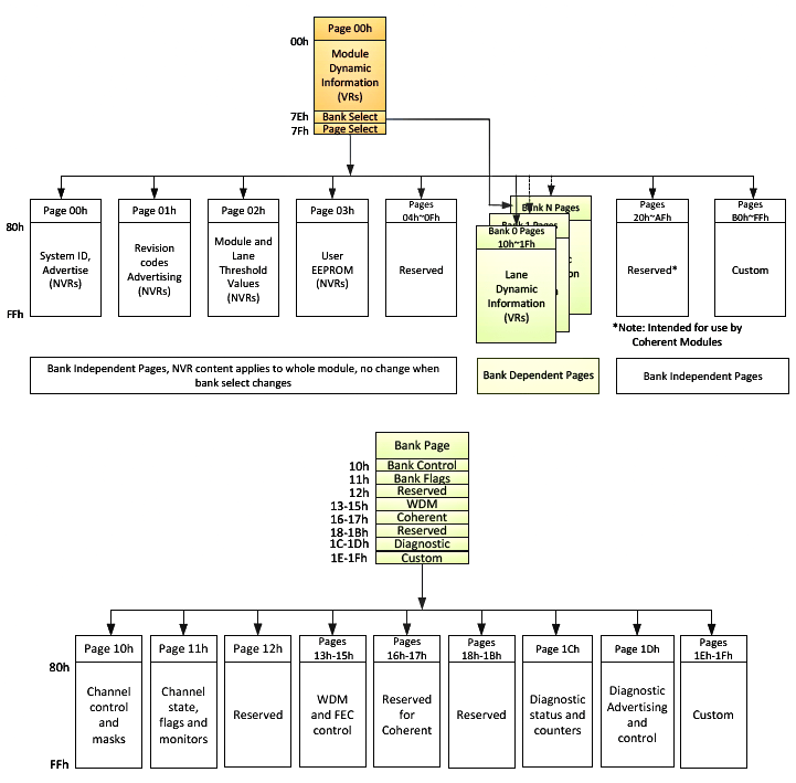
Figure 5. Mechanical Specifications
Regulatory Compliance
F-tone Networks FTQD-2H-LR8 transceivers are Class 1 Laser Products.
| Feature | Standard |
|---|---|
| Laser Safety | IEC 60825-1:2014 (Third Edition) |
| Environmental Protection | 2011/65/EU (RoHS) |
| CE EMC | EN55032:2015, EN55024:2010+A1:2015, EN61000-3-2:2014, EN61000-3-3:2013 |
| FCC | FCC Part 15, Subpart B; ANSI C63.4-2014 |
| Product Safety | EN/UL 60950-1, 2nd Edition, 2014-10-14 |
CAUTION: Use of controls or adjustments or performance of procedures other than those specified herein may result in hazardous radiation exposure.
Additional Product Images
Ordering Information
| Part Number | Product Description |
|---|---|
| FTQD-2H-LR8 | QSFP DD, 2x100GBASE-LR4, Duplex LC, up to 10km G.652 SMF |
Product Line Declaration
本产品为【200G QSFPDD LR8光收发模块 FTQD-2H-LR8】产品线,详细信息,请联系我们的销售人员,谢谢!
Important Notice
Performance figures, data and any illustrative material provided in this data sheet are typical and must be specifically confirmed in writing by F-tone Networks before they become applicable to any particular order or contract. In accordance with the F-tone Networks policy of continuous improvement specifications may change without notice. The publication of information in this data sheet does not imply freedom from patent or other protective rights of F-tone Networks or others. Further details are available from any F-tone Networks sales representative.